PCB manufacturing PCB manufacturing
Home > Blog

What Is Flux Soldering? Materials, PCB Uses, and Quality Tips

June 9th, 2026

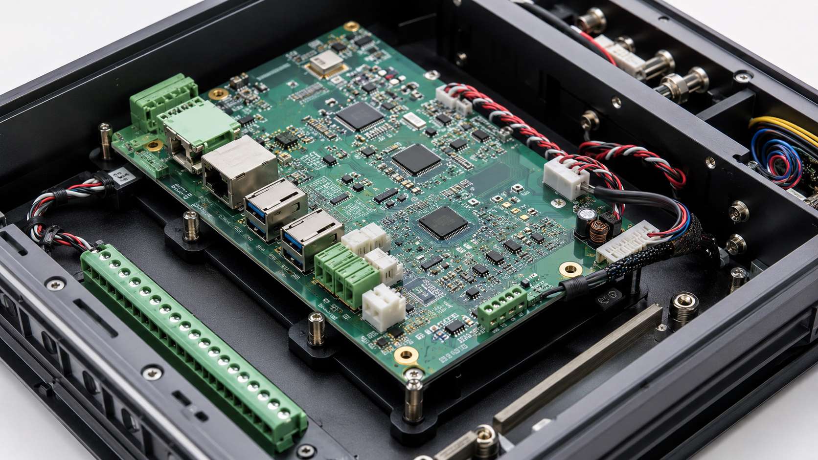
Flux soldering is the process of using soldering flux during soldering to clean metal surfaces, remove oxides, improve wetting, and help molten solder form a stable electrical and mechanical connection. In electronics, flux is not a small accessory. It directly affects solder joint appearance, conductivity, reliability, residue cleanliness, and long-term PCB performance.

For circuit boards, wire harnesses, connectors, sensors, power modules, and electronic assemblies, the right flux and solder combination can reduce cold joints, solder bridges, poor wetting, corrosion risk, and rework cost. A good solder joint is not made by heat alone. It needs clean metal, proper solder alloy, suitable flux activity, controlled temperature, correct dwell time, and reliable inspection.

What Is Flux Soldering?

Flux soldering means soldering with the help of flux, a chemical material that prepares copper pads, component leads, wires, terminals, or plated surfaces before molten solder bonds to them. The basic definition of soldering is the joining of metal surfaces by melting a filler metal called solder, while the base metals themselves do not melt.

In electronics, the solder usually melts at a lower temperature than copper, nickel, tin plating, or component terminals. Flux works during heating. It removes thin oxide layers, protects the hot metal from fresh oxidation, and helps solder spread instead of balling up. This spreading behavior is called wetting.

Without flux, solder may sit on the pad like a bead of water on wax. With the right flux, solder flows across the pad, climbs the component lead, and forms a smooth fillet. This is why flux for electrical soldering is essential in PCB assembly, hand soldering, wave soldering, selective soldering, rework, and repair.

What Is Flux Soldering?

Why Is Flux Important for Electrical Soldering?

The purpose of flux for soldering is simple but critical: it helps solder bond to metal. Copper, tin, nickel, silver, and other solderable finishes react with oxygen in the air. Even when a pad looks clean, a very thin oxide film may already be present. During soldering, heat makes oxidation faster.

Flux supports electrical soldering in several important ways:

  • It removes oxide from PCB pads, component leads, wires, and terminals.
  • It helps molten solder spread evenly across the metal surface.
  • It reduces the risk of poor wetting, cold joints, and weak connections.
  • It protects the hot soldering area from fresh oxidation during heating.
  • It improves solder joint consistency in hand soldering and mass production.
  • It helps reduce rework cost when the process is properly controlled.

For production engineers, flux selection also affects process yield. A flux that is too weak may cause non-wetting or insufficient hole fill. A flux that is too aggressive may leave residues that require cleaning. A flux used in excess may create ionic contamination, coating adhesion issues, or leakage risk in humid environments.

How Does Flux Soldering Work?

Flux soldering works through heat-activated chemistry. At room temperature, many fluxes are relatively stable. As the soldering iron, reflow oven, selective soldering nozzle, or wave solder pot heats the joint area, the flux activates and begins to remove oxide from the metal surface.

A typical flux soldering process works like this:

  • The PCB pad, wire, terminal, or component lead is heated.
  • Flux becomes active as the temperature rises.
  • The activated flux removes oxide and surface contamination.
  • Molten solder reaches the cleaned metal surface.
  • Solder wets the pad and component lead.
  • A metallic bond forms between solder and the solderable surface.
  • The joint cools and solidifies into a stable connection.
How Does Flux Soldering Work?

The key point is that flux does not replace proper heat. It supports proper heat transfer and wetting. Too little heat leaves the joint dull, grainy, or poorly bonded. Too much heat can burn flux, lift pads, damage components, or create excessive intermetallic growth. Good flux soldering is a balance between chemistry, temperature, time, surface finish, and solder alloy.

What Is Solder Made Of?

Solder is a metal alloy used to join conductive surfaces. In electronics, solder is commonly made of tin-based alloys because tin wets copper and many plated finishes well. Traditional leaded solder often used tin and lead, such as Sn63/Pb37. Modern lead-free solder often uses tin, silver, and copper, such as SAC305.

Common solder materials include:

  • Tin: the main base metal in many electronic solders.
  • Lead: used in traditional tin-lead solder where permitted.
  • Silver: improves mechanical strength and thermal fatigue resistance in some lead-free alloys.
  • Copper: helps control copper dissolution and supports lead-free solder performance.
  • Bismuth: often used in low-temperature solder.
  • Antimony: sometimes used in higher-temperature solder alloys.
  • Indium: used in some special low-temperature or high-reliability applications.
Solder TypeTypical CompositionCommon UseKey Point
Sn63/Pb3763% tin, 37% leadLegacy electronics, repair where permittedEutectic alloy with sharp melting behavior
SAC305Tin, 3% silver, 0.5% copperLead-free PCB assemblyWidely used in SMT and reflow soldering
Sn99.3/Cu0.7Tin-copperWave soldering, cost-sensitive lead-free assemblyLower cost than silver-bearing alloys
Sn42/Bi58Tin-bismuthLow-temperature solderingUseful for heat-sensitive parts
High-temperature solderTin-antimony, gold-tin, or special alloysPower, hybrid, ceramic, and staged assemblySelected for higher service or process temperatures

A common buyer question is: what is high heat solder called in electrical applications? In electronics, people may call it high-temperature solder, high-melting-point solder, or high-temp solder. The exact alloy depends on the process. For example, gold-tin may be used in some high-reliability or hermetic applications, while tin-antimony may appear in certain power or thermal applications.

What Materials Are Commonly Used in Solder and Flux?

Solder and flux are different materials, but they work together. Solder provides the metal connection. Flux provides the chemical cleaning and wetting support.

Common solder materials include:

  • Tin-based alloys for most PCB assembly work.
  • Tin-lead alloys for legacy or exempted applications.
  • Tin-silver-copper alloys for lead-free SMT assembly.
  • Tin-copper alloys for some wave soldering processes.
  • Tin-bismuth alloys for low-temperature soldering.
  • Special high-temperature alloys for power, ceramic, hybrid, or staged soldering.

Common flux materials may include:

  • Rosin or resin.
  • Organic acid activators.
  • Solvents.
  • Thixotropic agents.
  • Wetting promoters.
  • Stabilizers and other process additives.

In PCB assembly, flux chemistry should be matched with the soldering method, surface finish, component type, cleaning capability, and reliability class. A product used in consumer lighting does not always need the same flux system as a medical control board, aerospace module, industrial sensor, or automotive electronic assembly.

What Are the Main Types of Soldering Techniques Used in Electronics?

The main types of soldering techniques used in electronics include hand soldering, reflow soldering, wave soldering, selective soldering, drag soldering, hot air rework, laser soldering, and robotic soldering. Each process uses flux differently.

TechniqueTypical ApplicationFlux UseEngineering Note
Hand solderingRepair, prototyping, wires, connectorsFlux-cored wire, liquid flux, rosin flux pasteOperator skill strongly affects quality
Reflow solderingSMT componentsFlux inside solder pasteProfile control is critical
Wave solderingThrough-hole assemblySpray or foam flux before waveFlux coverage and preheat matter
Selective solderingLocal through-hole solderingTargeted flux applicationGood for mixed SMT/THT boards
Hot air reworkIC replacement, SMD repairGel flux or tacky fluxAvoid overheating nearby parts
Drag solderingFine-pitch IC leadsLiquid or gel fluxFlux helps prevent bridging
Robotic solderingRepeatable jointsWire core plus extra flux if neededTip condition and feed rate matter

For small-batch PCB prototype assembly, hand soldering and reflow are common. For medium and high-volume production, reflow plus wave or selective soldering is often used. For dense PCBA with BGA, QFN, and fine-pitch connectors, flux residue, voiding, wetting, and thermal profiling become more important.

What Are the Main Solder Types and Flux Types?

Solder types are usually grouped by alloy and form. Flux types are usually grouped by chemistry, activity level, and residue behavior.

Common solder forms include:

  • Solder wire for hand soldering and repair.
  • Solder paste for SMT reflow assembly.
  • Solder bar for wave soldering pots.
  • Solder preforms for controlled solder volume.
  • Solder balls for BGA and advanced package assembly.
  • Solder rings for selected terminal or connector applications.

Common flux types include:

Flux TypeTypical UseAdvantageLimitation
Rosin fluxHand soldering, repair, electronicsStable, familiar, good wettingMay require cleaning depending on type
RMA fluxGeneral electronicsMild activation with good process windowResidues must be assessed
No-clean fluxSMT, selective soldering, many production boardsLower cleaning costOveruse can still cause residue issues
Water-soluble fluxHigh-activity solderingStrong cleaning actionMust be cleaned thoroughly
Tacky gel fluxRework, BGA, QFN, fine-pitch ICsStays in placeResidue management needed
Liquid fluxWave soldering, selective soldering, hand applicationEasy coverageApplication control is important

For most electronic circuit boards, acid-core plumbing flux should not be used. It can leave corrosive residues and damage copper, pads, component leads, and insulation resistance over time. Electronics requires flux designed for electrical soldering, not pipe joining.

Does Solder Conduct Electricity?

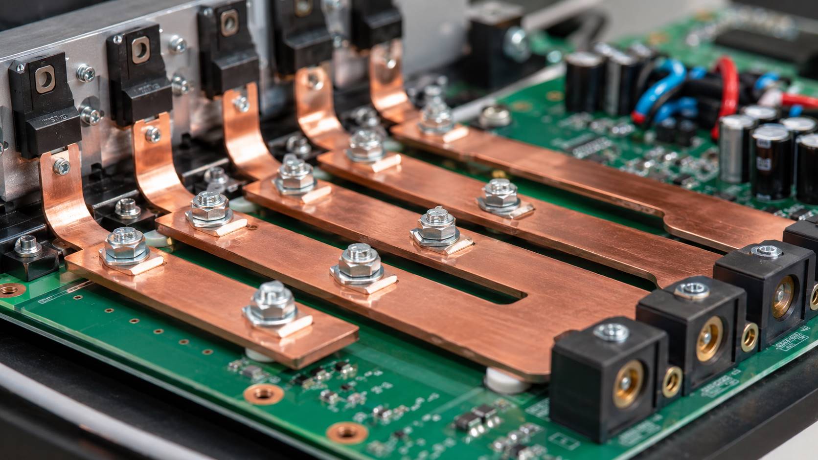
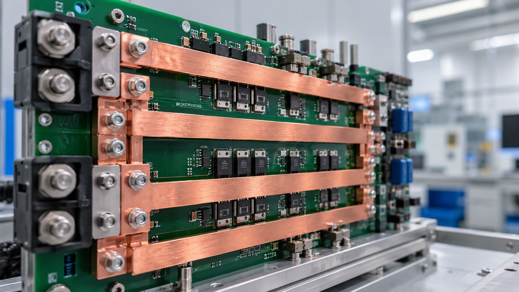
Yes, solder conducts electricity. That is one reason it is used in electronics. However, solder is not as conductive as copper. The PCB trace, pad, via barrel, and component termination provide the main conductive structure, while solder forms the joining bridge.

This matters in high-current designs. A solder joint should not be treated as a large copper busbar unless the current path, cross-sectional area, heat rise, and mechanical stress have been reviewed.

For power-related PCB designs, engineers should also consider:

  • Copper weight.
  • Pad size.
  • Via quantity and via diameter.
  • Connector structure.
  • Terminal plating.
  • Solder joint geometry.
  • Heat dissipation path.
  • Mechanical vibration and stress.

In practical terms, solder conducts electricity well enough for normal component joints. But joint geometry, wetting quality, voids, cracks, and contamination can affect real performance. A shiny joint that looks acceptable may still need X-ray, cross-section, pull testing, ICT, or functional testing if the product is safety-critical or high-reliability.

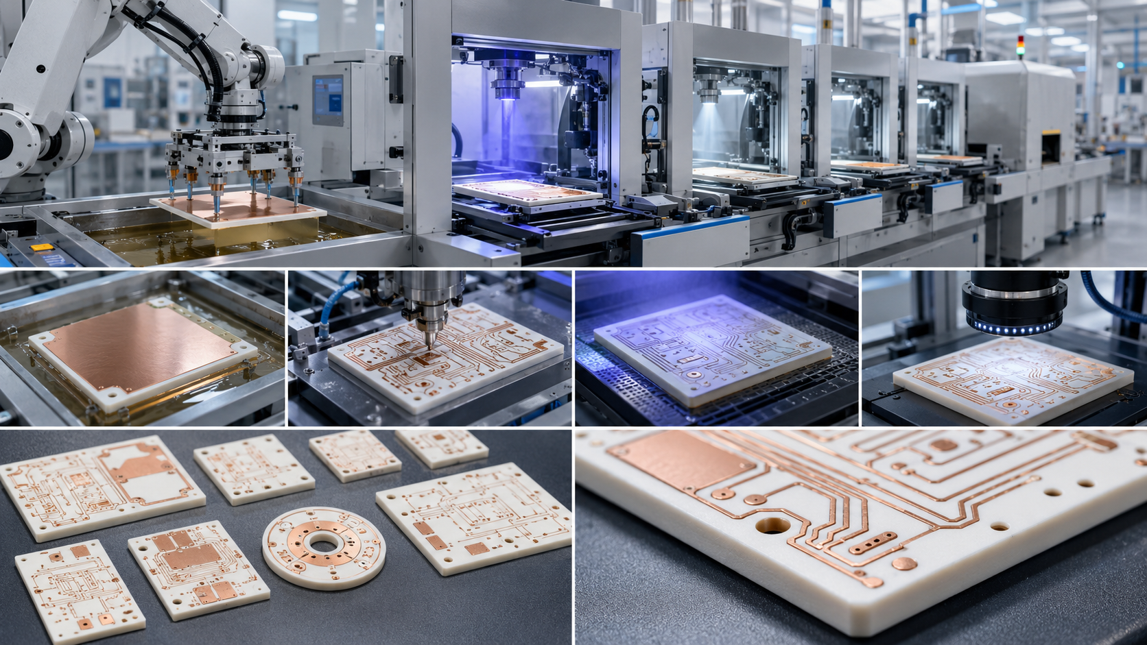
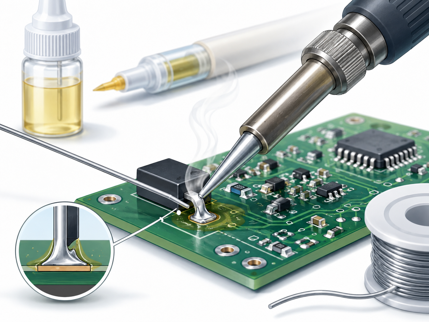
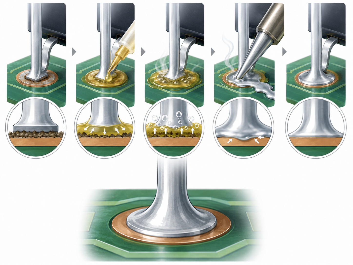
How to Use Soldering Flux on a Circuit Board

To use soldering flux on a circuit board, apply a small amount to the pad, lead, or joint area before heating. The goal is controlled coverage, not flooding the board. Excess flux can spread under components, collect around connectors, or create cleaning challenges.

A practical soldering workflow is:

  • Prepare the soldering area: Make sure PCB pads, component leads, wires, or terminals are clean and solderable.
  • Apply a small amount of flux: Use a flux pen, syringe, brush, or paste. Avoid excessive flux.
  • Heat the pad and lead together: The soldering iron tip should contact both metal surfaces, not only the solder wire.
  • Feed solder into the heated joint: Add solder to the joint area, allowing it to melt and flow naturally.
  • Allow solder to wet both surfaces: A good joint should form a smooth fillet and cover the pad properly.
  • Remove solder first, then remove heat: This helps control solder volume and joint shape.
  • Keep the joint still while cooling: Movement during cooling may create a disturbed or weak joint.
  • Inspect the solder joint: Check for bridges, insufficient solder, poor wetting, cracks, and residue.
StepActionWhat to Watch
Prepare the surfaceConfirm pads and leads are cleanOxidized parts may need stronger flux or replacement
Apply fluxUse flux pen, syringe, brush, or pasteAvoid excessive volume
Heat the jointTouch both pad and lead with the iron tipHeat the work, not only the solder
Feed solderAdd solder to the heated joint areaDo not melt solder only on the tip
Let it flowAllow solder to wet both surfacesGood wetting forms a smooth fillet
Remove heatHold the joint still while coolingMovement can cause disturbed joints
InspectCheck shape, coverage, bridges, residueClean if required by process

For how to solder to a circuit board, the most important habit is to heat the pad and lead together, then feed solder into the joint. If solder melts on the iron tip but does not wet the pad, the pad may be cold, oxidized, contaminated, or missing enough flux.

How to Use Rosin Flux Paste?

Rosin flux paste is popular for hand soldering, repair, wires, connectors, and some rework tasks. It is helpful when reworking old boards, tinning wires, soldering larger terminals, or repairing joints that no longer wet properly.

A practical way to use rosin flux paste is:

  • Take a very small amount of rosin flux paste with a clean tool, syringe, brush, or toothpick.
  • Place it only on the pad, lead, wire, or terminal that needs soldering.
  • Heat the pad and lead with a clean soldering iron tip.
  • Feed solder when the joint area is hot enough.
  • Let the solder flow across the metal surface.
  • Remove excess residue if your process requires cleaning.

Rosin flux paste can also help with drag soldering fine-pitch ICs because it improves solder flow and reduces bridging. The mistake is using too much. Thick flux residue may look harmless, but it can trap debris, affect coating adhesion, or complicate inspection.

For high-reliability assemblies, cleaning and residue validation should follow the customer requirement, product class, and internal process control plan.

How to Use the Soldering Iron Correctly

Using the soldering iron correctly is just as important as choosing flux. A good soldering iron should have stable temperature control, suitable power, correct tip shape, and proper grounding for ESD-sensitive electronics.

Good soldering iron habits include:

  • Use a suitable tip size for the pad and component lead.
  • Keep the soldering tip clean and lightly tinned.
  • Heat both the PCB pad and component lead at the same time.
  • Avoid melting solder only on the iron tip.
  • Use enough heat transfer, not excessive temperature.
  • Remove heat as soon as the joint is properly formed.
  • Avoid pressing hard on PCB pads, especially small SMD pads.
  • Replace oxidized or damaged soldering tips in time.

For most PCB hand soldering, a chisel tip often works better than a needle tip because it transfers heat more efficiently. A very tiny tip may look precise, but it can lack thermal mass.

Temperature depends on solder alloy, board thickness, copper area, component size, and dwell time. Lead-free solder usually needs higher working temperature than tin-lead solder. However, turning the iron too high is not a true solution. Excess temperature burns flux quickly, damages pads, and reduces process control.

How to Choose Solder Sizes, Wire Diameter, and Flux Form

Solder sizes affect control. For fine PCB work, thin solder wire gives better volume control. For large terminals, thicker wire improves feeding speed. For SMT production, solder paste particle size and stencil aperture design affect paste release, bridging, tombstoning, and joint volume.

Common hand soldering wire choices include:

  • 0.3 mm solder wire: Suitable for fine-pitch SMD parts, small pads, jumper wires, and precise repair.
  • 0.5 mm solder wire: Suitable for general PCB repair, small through-hole parts, and moderate SMD work.
  • 0.8 mm solder wire: Suitable for through-hole resistors, capacitors, headers, and common hand soldering tasks.
  • 1.0 mm or thicker solder wire: Suitable for larger terminals, wires, shields, connectors, and high solder volume areas.

Flux form should also follow the actual soldering job:

  • Flux pen: clean and convenient for small PCB areas.
  • Liquid flux: suitable for broad coverage, wave soldering, selective soldering, and repair.
  • Gel flux: useful for rework because it stays where placed.
  • Rosin flux paste: practical for wires, terminals, and repair jobs.
  • Solder paste: used for SMT because it combines solder powder and flux.
  • Flux-cored solder wire: convenient for hand soldering and maintenance.

The best choice depends on pad size, component type, soldering method, operator skill, cleaning requirement, and final reliability target.

What Are the Advantages and Limits of Flux Soldering?

Flux soldering brings several clear advantages, especially in electronics manufacturing and PCB assembly.

Main advantages include:

  • Better solder wetting on copper pads and component leads.
  • Lower risk of cold joints and non-wetting.
  • Smoother solder flow during hand soldering and rework.
  • Easier fine-pitch soldering when used properly.
  • Improved solder joint consistency in production.
  • Lower rework rate when flux, heat, and solder are well controlled.
  • Better support for old, slightly oxidized, or difficult-to-solder surfaces.

However, flux soldering also has limits.

Common limitations include:

  • Flux cannot fix a badly damaged PCB pad.
  • Flux cannot fully solve poor surface finish or severe oxidation.
  • Flux cannot compensate for the wrong solder alloy.
  • Flux cannot replace proper heat transfer.
  • Excess flux can leave residue and cleaning problems.
  • Strong flux may require strict cleaning after soldering.
  • No-clean flux still needs process control and validation.
  • Burned flux can reduce solderability and make rework harder.

No-clean flux does not mean “no residue exists.” It means the residue is designed to be benign under defined conditions. If too much flux is used, if it is not fully activated, or if the assembly works in humid, high-voltage, high-impedance, or coated environments, residue control becomes important.

Common Flux Soldering Defects and Failure Analysis

Many soldering defects are related to flux activity, heat transfer, surface condition, or process control. The root cause is rarely one single factor.

DefectPossible CausePractical Fix
Cold jointLow heat, movement, poor wettingIncrease heat transfer, stabilize joint, use proper flux
Non-wettingOxidized pad, weak flux, contaminated finishCheck surface finish, flux activity, storage condition
Solder bridgeToo much solder, excess flux, fine pitch spacingUse less solder, drag technique, solder wick, correct flux
Solder ballingPoor paste control, excessive flux, bad profileReview stencil, reflow profile, paste storage
Insufficient hole fillPoor preheat, weak flux, thermal imbalanceImprove flux coverage and thermal profile
Flux residueOver-application, wrong flux, incomplete cleaningControl volume, validate cleaning process
CorrosionAggressive flux residue, poor cleaningUse electronics-grade flux and verify cleanliness
Intermittent connectionCracked joint, poor wetting, vibrationImprove pad design, solder volume, mechanical support

Typical engineering findings include:

  • If the solder joint looks dull and rough, the cause may be low heat, movement during cooling, or poor wetting.
  • If solder balls appear around SMT pads, the issue may relate to solder paste printing, reflow profile, flux behavior, or board contamination.
  • If through-hole solder does not fill the barrel, flux coverage, preheat, copper thermal mass, and hole-to-lead ratio should be checked.
  • If fine-pitch IC leads keep bridging, excessive solder volume or poor drag soldering technique may be the real problem.
  • If residue appears after soldering, flux type, application volume, activation temperature, and cleaning process should be reviewed.

A common production case is connector soldering on thick copper PCBs. The operator adds more solder, but the joint still looks rough. The real issue may be insufficient heat transfer because the copper plane pulls heat away. Better tip size, preheating, controlled flux, and pad thermal design solve the issue more effectively than simply increasing solder volume.

Another case is fine-pitch IC bridging. Adding more heat can make bridging worse. A small amount of gel flux, clean tip, controlled drag soldering, and solder wick usually give a cleaner result.

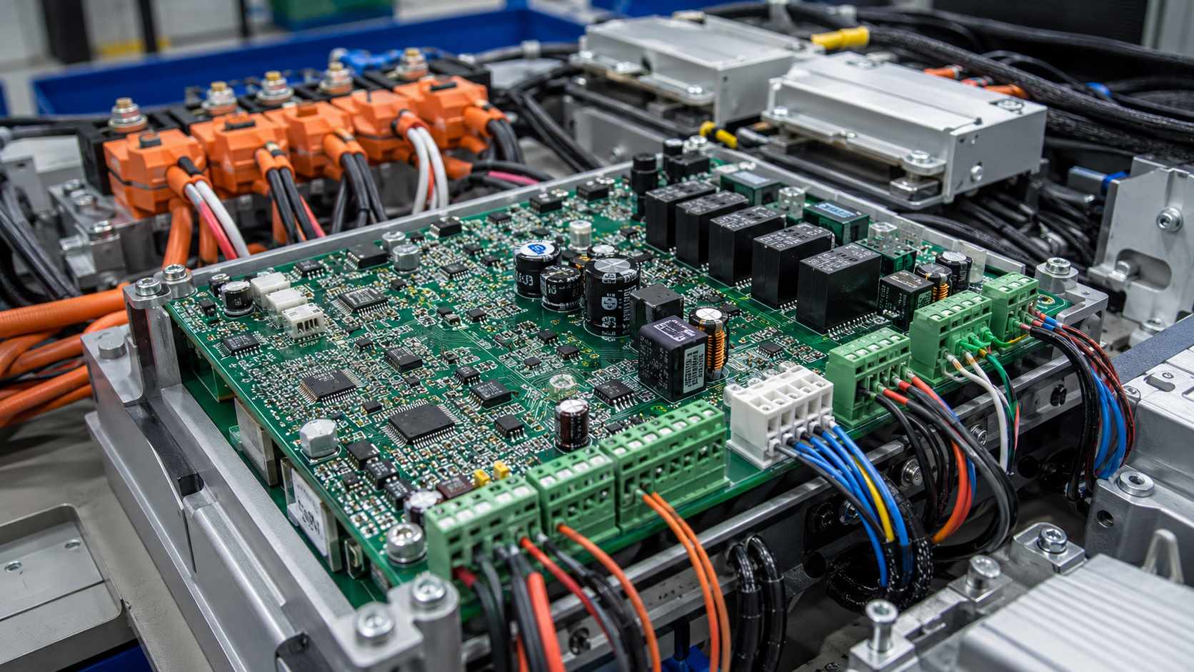
Where Is Flux Soldering Used in Electronics Manufacturing?

Flux soldering is used almost everywhere electronic interconnections are made. It appears in consumer electronics, industrial control boards, automotive electronics, medical devices, communication equipment, LED lighting, power supplies, sensors, robotics, aerospace-related electronics, and new energy products.

Common application areas include:

  • SMT assembly for resistors, capacitors, ICs, QFNs, BGAs, and connectors.
  • Through-hole soldering for headers, transformers, switches, and terminals.
  • Wire tinning and wire-to-board soldering.
  • Connector and cable assembly.
  • PCB repair and component replacement.
  • BGA and QFN rework.
  • LED PCB assembly.
  • Power electronics soldering.
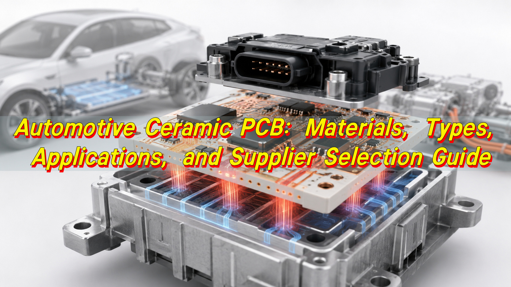
  • Ceramic PCB and metal-core PCB assembly.
  • Industrial control board manufacturing.
  • Medical and automotive electronic modules.

In SMT assembly, flux is inside solder paste. In through-hole assembly, flux is applied before wave or selective soldering. In repair, technicians use liquid flux, gel flux, or rosin paste to restore wetting. In cable and wire harness work, flux helps tin stranded wires and solder terminals.

For medical, automotive, aerospace, and industrial control projects, flux soldering is not only an operator skill. It is a controlled manufacturing process. Material lot control, solder paste storage, stencil printing, reflow profiling, cleaning validation, AOI, X-ray, ICT, and functional testing all contribute to final reliability.

How to Select Flux and Solder for a PCB Project?

A good selection starts with the product requirement, not the flux catalog. Engineers should review the application environment, PCB finish, component plating, assembly method, cleaning capability, operating voltage, current load, humidity exposure, coating requirement, and regulatory target.

Key selection factors include:

  • PCB surface finish: ENIG, HASL, OSP, immersion silver, immersion tin, or other finishes.
  • Soldering process: hand soldering, reflow, wave, selective soldering, or rework.
  • Component type: SMD, through-hole, BGA, QFN, connector, wire, or terminal.
  • Temperature sensitivity: especially for plastic connectors, sensors, LEDs, and special modules.
  • Cleaning requirement: no-clean, water cleaning, solvent cleaning, or validated residue control.
  • Reliability class: consumer, industrial, medical, automotive, aerospace-related, or high-power.
  • Compliance target: RoHS, customer specification, IPC workmanship requirement, or internal standard.
  • Operating environment: humidity, vibration, high voltage, high current, thermal cycling, or coating.

For general lead-free SMT, SAC305 solder paste with a qualified no-clean flux is common. For cost-sensitive through-hole wave soldering, tin-copper alloy may be considered. For heat-sensitive components, low-temperature bismuth-based solder may reduce thermal stress. For high-reliability assemblies, the solder and flux system should be validated through process trials and reliability testing.

What Should Buyers Ask Before Choosing a Soldering Supplier?

Buyers should not only ask whether the supplier can solder the PCB. They should ask how the soldering process is controlled. This is especially important for OEM manufacturing, ODM production, prototype assembly, and batch PCBA projects.

Useful questions include:

  • Which solder alloy will be used for this project?
  • Which flux type or solder paste brand is selected?
  • Is the flux compatible with the PCB surface finish?
  • Is the process lead-free and RoHS compliant if required?
  • Is cleaning required after soldering?
  • Can the supplier provide a reflow profile?
  • Will AOI or X-ray inspection be used?
  • How are BGA, QFN, or hidden solder joints inspected?
  • How are solder paste storage and thawing controlled?
  • How are hand soldering and rework operations managed?
  • Can the factory provide ICT, FCT, or custom test support?
  • Are soldering defects recorded and analyzed during production?
  • Can the supplier support prototype, small batch, and mass production?

For overseas buyers sourcing from a China-based PCB or PCBA factory, the most useful approach is not asking for the cheapest soldering option. It is asking for a process-matched solution that fits product risk, target market, quantity, test requirement, and long-term reliability.

Cost Factors in Flux Soldering and PCB Assembly

Flux soldering cost is influenced by solder alloy, flux type, assembly complexity, cleaning requirement, inspection method, production volume, and reliability class. Silver-bearing solder such as SAC305 usually costs more than tin-copper solder. Water-soluble flux may require cleaning equipment, DI water control, drying, and cleanliness verification. High-reliability assemblies may need extra testing.

Main cost factors include:

  • Solder alloy cost.
  • Flux type and solder paste grade.
  • PCB surface finish.
  • SMT component density.
  • Through-hole soldering quantity.
  • BGA, QFN, or fine-pitch assembly difficulty.
  • Manual soldering and rework time.
  • Cleaning process requirement.
  • AOI, X-ray, ICT, and FCT coverage.
  • Prototype quantity or mass production volume.
  • Reliability testing requirement.
  • Documentation and traceability level.

The largest hidden cost is rework. Poor wetting, bridging, insufficient solder, tombstoning, or contamination can consume more money than the original solder material. For B2B procurement, the cheapest flux or solder paste may increase total cost if it causes unstable yield.

PCB design also affects cost. Large copper planes, heavy copper layers, tight pad spacing, poor thermal relief, difficult connectors, and mixed large-small components may require more process tuning. A manufacturer with strong DFM review can identify these risks before production, reducing repeated trial runs and urgent rework.

Quality Control, Testing Methods, and Standards

Quality control for flux soldering should cover incoming materials, process setup, operator control, inspection, cleaning, and final testing. Solder paste should be stored and thawed according to supplier requirements. Flux should be controlled by lot, shelf life, solids content, and application method. Reflow ovens should be profiled with real boards, not only generic settings.

Common quality control points include:

  • Solder paste storage and thawing records.
  • Flux shelf life and lot traceability.
  • PCB surface finish inspection.
  • Component solderability control.
  • Stencil printing quality.
  • SPI inspection for solder paste volume.
  • Reflow temperature profile verification.
  • Wave or selective soldering preheat control.
  • Hand soldering operator training.
  • AOI inspection after soldering.
  • X-ray inspection for hidden solder joints.
  • Cleaning process validation when needed.
  • Ionic contamination or SIR testing for high-reliability boards.
  • ICT and FCT for electrical and functional verification.

Common inspection and test methods include:

  • Visual inspection.
  • AOI inspection.
  • X-ray inspection.
  • Solderability testing.
  • Cross-section analysis.
  • Ionic contamination testing.
  • Surface insulation resistance testing.
  • ICT testing.
  • FCT functional testing.
  • Pull testing.
  • Thermal cycling when required.

For products entering the EU or markets with similar compliance expectations, RoHS material control should also be considered. For industrial, medical, automotive, and aerospace-related products, soldering quality should be managed as a complete process, not only as a final appearance check.

Global Procurement Tips for OEM and ODM Electronics Projects

When sourcing soldered PCB assemblies from a China source factory, overseas buyers should focus on real process capability instead of virtual local claims. A reliable supplier should explain the solder alloy, flux system, cleaning policy, inspection plan, and test coverage clearly.

For North American and European buyers, the main concerns are often:

  • Compliance documentation.
  • Traceability.
  • Stable batch quality.
  • IPC workmanship control.
  • Long-term reliability.
  • Clear engineering communication.
  • Consistent soldering process.
  • Functional testing and inspection records.

For Southeast Asian and fast-growing hardware teams, common priorities may include:

  • Flexible MOQ.
  • Fast sample development.
  • Cost control.
  • Engineering feedback.
  • Small-batch trial production.
  • Smooth transition to mass production.

Before placing an order, prepare these files and requirements:

  • Gerber files.
  • BOM.
  • Pick-and-place file.
  • Assembly drawing.
  • PCB stack-up if needed.
  • Soldering requirements.
  • Test plan.
  • Conformal coating requirement if any.
  • Special notes for connectors, wires, high-current pads, or heat-sensitive components.
  • Packaging and labeling requirements.
  • Target market compliance requirements.

If the product has medical, automotive, aerospace-related, high-current, high-voltage, or harsh-environment use, state that early. The supplier can then select a more suitable soldering process, flux system, inspection route, and documentation package.

FAQ

1. What is flux soldering in simple words?

Flux soldering is soldering with a chemical helper called flux. The flux cleans the metal surface, removes oxide, and helps melted solder flow smoothly onto PCB pads, wires, or component leads. In electronics, flux helps create a stronger and more reliable joint than heat and solder alone.

2. What is the purpose of flux for soldering?

The purpose of flux for soldering is to remove oxidation, improve wetting, and protect the hot metal surface while solder is flowing. Without flux, solder may bead up, fail to spread, or form a weak joint. Flux is especially important on copper pads, old boards, fine-pitch leads, and through-hole terminals.

3. What is electrical soldering flux?

Electrical soldering flux is flux made for electronic and electrical connections. It is different from plumbing flux. Electronics-grade flux is designed to support solderability while reducing corrosion and contamination risk when used correctly. Common forms include flux pens, liquid flux, rosin paste, gel flux, and flux inside solder wire or solder paste.

4. How do you use soldering flux on a PCB?

Apply a small amount of flux to the pad and component lead, heat both surfaces with a clean soldering iron tip, then feed solder into the joint. Let solder flow naturally across the pad and lead. After cooling, inspect the joint. Clean residues if your process or product requirement calls for cleaning.

5. How do you use rosin flux paste?

Use a small amount of rosin flux paste on the joint area before heating. It is useful for wires, connectors, repair work, and oxidized pads. Do not cover the board with excessive paste. After soldering, inspect the residue and clean it when required by the product class, coating process, or customer specification.

6. What is solder made of?

Solder is usually made of tin-based metal alloys. Traditional solder may contain tin and lead, while modern lead-free solder often contains tin, silver, and copper. Other solder types may include bismuth, antimony, indium, or special alloys. The right alloy depends on melting temperature, reliability, compliance, and application.

7. Does solder conduct electricity?

Yes, solder conducts electricity, but copper conducts better. In a PCB, solder mainly creates the connection between the component termination and copper pad. For high-current designs, engineers should not rely only on solder volume. Pad size, copper thickness, vias, terminals, and thermal design must also be considered.


Tantalum Capacitor vs Electrolytic: Which One Should You Use?

June 9th, 2026

When comparing tantalum capacitor vs electrolytic, the key choice is whether your PCB needs compact stability or stronger bulk power filtering. Tantalum capacitors are better for small, stable, low-voltage rails, while aluminum electrolytic capacitors are better for high capacitance, high ripple current, and cost-sensitive power circuits.

For PCB and PCBA projects, do not select a capacitor by capacitance value only. Check ESR, leakage current, rated voltage, voltage derating, ripple current, temperature grade, package size, polarity, soldering process, and supply stability before approving the part.

Tantalum Capacitor vs Electrolytic.

What Is a Tantalum Capacitor?

A tantalum capacitor is a polarized electrolytic capacitor made with a tantalum anode and tantalum pentoxide dielectric. It is used when a PCB needs high capacitance in a small package.

Tantalum capacitors are common in compact PCB assemblies, IoT modules, communication boards, medical electronics, portable devices, and stable low-voltage power rails. Their main strengths are small size, stable capacitance, low leakage current, and good performance density.

The main risk is electrical stress. Tantalum capacitors are sensitive to reverse polarity, voltage spikes, surge current, hot-plug input, and poor derating. They work best on regulated rails, not directly on unstable raw power inputs.

What Is an Electrolytic Capacitor?

An electrolytic capacitor is a polarized capacitor used for high capacitance, filtering, smoothing, and energy storage. In most PCB discussions, it usually refers to an aluminum electrolytic capacitor.

Aluminum electrolytic capacitors are widely used in power supplies, LED drivers, adapters, motor control boards, chargers, inverters, audio circuits, and industrial electronics. Their main strengths are large capacitance, higher voltage options, strong bulk filtering, and lower cost per µF.

Their limits are also clear. Aluminum electrolytic capacitors are usually larger, and their ESR, leakage current, capacitance stability, and lifetime can be affected by heat, ripple current, electrolyte drying, and long operating time.

Are Tantalum Capacitors the Same as Electrolytic Capacitors?

Tantalum capacitors are a type of electrolytic capacitor, but they are not the same as common aluminum electrolytic capacitors. In practical comparison, tantalum capacitor vs electrolytic usually means tantalum capacitor vs aluminum electrolytic capacitor.

Both types are usually polarized and can be used for filtering, smoothing, decoupling, and energy storage. The differences are material, dielectric structure, electrolyte system, ESR, leakage current, ripple current, size, cost, and failure mode.

The simple conclusion is this: tantalum is usually smaller and more stable, while aluminum electrolytic is usually cheaper and better for high capacitance and high ripple current applications.

Tantalum Capacitor vs Electrolytic: What Is Difference?

The main difference in tantalum capacitor vs electrolytic selection is compact stability versus bulk power capacity. Tantalum capacitors fit compact low-voltage rails, while aluminum electrolytic capacitors fit larger capacitance and power filtering positions.

The values below are common engineering ranges. Actual values depend on brand, series, voltage rating, case size, temperature grade, and application conditions.

ParameterTantalumAluminum Electrolytic
Capacitance Range0.1µF–1,500µF common0.47µF–100,000µF+ common
Rated Voltage2.5V–50V common6.3V–450V common
ESR10mΩ–5Ω depending on type20mΩ–several Ω depending on size
Leakage CurrentOften below 0.01CVOften 0.01CV–0.03CV
Ripple CurrentTens of mA to several AHundreds of mA to several A+
Temperature Range-55°C to +125°C common-40°C to +105°C / +125°C common
LifetimeLong with proper derating1,000–10,000+ hours rated
Package SizeCompact SMD commonRadial, SMD, snap-in, larger sizes
Surge ToleranceSensitive to surge currentBetter in many input circuits
CostHigher per µFLower per µF

Do not choose by capacitance value alone. A capacitor near an IC pin, DC input, switching regulator, or bulk power rail may require different ESR, ripple current, voltage margin, and package limits.

Tantalum Capacitor vs Electrolytic: Which One Is More Stable?

Tantalum capacitors are usually more stable in capacitance, leakage current, and long-term electrical behavior. They are better for stable low-voltage rails, compact layouts, and low-leakage circuits.

Aluminum electrolytic capacitors are less stable over long use because heat and ripple current can dry the electrolyte and increase ESR. However, they can handle rough input filtering better when rated correctly.

For stable regulated rails, choose tantalum. For rough input filtering, high capacitance, or high ripple current, choose aluminum electrolytic. This is one of the most important engineering rules in a tantalum capacitor vs electrolytic decision.

Tantalum Capacitor vs Electrolytic: ESR, Leakage Current and Electrical Performance

Tantalum capacitors usually have lower ESR and lower leakage current than standard aluminum electrolytic capacitors. This helps reduce ripple and improve local power rail stability.

ESR affects ripple voltage, heat, transient response, and regulator stability. Lower ESR is not always safer. Some regulators require a specific ESR range, and the wrong capacitor can cause oscillation or unstable startup.

ParameterTantalumAluminum Electrolytic
ESR Range10mΩ–5Ω common20mΩ–several Ω common
Leakage CurrentOften ≤0.01CVOften 0.01CV–0.03CV
Ripple CurrentTens of mA to several AHundreds of mA to several A+
Capacitance Tolerance±10%, ±20% common±20% common
Frequency UseLocal rail filteringBulk smoothing, low-frequency ripple
Voltage Derating50% margin often used20%–30% margin common
Temperature Grade+85°C, +105°C, +125°C+85°C, +105°C, +125°C
Impedance RangeLow to mediumMedium to high

For replacement, capacitance and voltage are not enough. Check ESR, leakage current, ripple current, impedance curve, temperature rating, and regulator requirements before changing capacitor type.

Tantalum Capacitor vs Electrolytic

Tantalum Capacitor vs Electrolytic: Which Is Better for Power Filtering?

Aluminum electrolytic capacitors are usually better for bulk power filtering and high ripple current. They are common at DC inputs, rectifier outputs, power supply outputs, LED drivers, motor control boards, and DC bus circuits.

Their larger case size supports higher capacitance and better heat dissipation. If ripple current is too high, the capacitor can overheat, dry out faster, lose capacitance, or fail early.

Use this rule:

  • Choose aluminum electrolytic for bulk capacitance, high ripple current, and lower cost.
  • Choose tantalum for compact size, stable local rails, and lower leakage.
  • Use ceramic capacitors for high-frequency decoupling near IC pins.
  • Check regulator ESR requirements before replacement.
  • Confirm ripple current with temperature rise testing.

Tantalum Capacitor vs Electrolytic: Which One Lasts Longer?

Tantalum capacitors can last longer in stable and well-derated circuits because solid tantalum types do not dry out like many aluminum electrolytic capacitors.

Aluminum electrolytic capacitors can also last long if selected with 105°C or 125°C rating, enough ripple current margin, and reliable brand quality. Their lifetime depends heavily on working temperature, ripple current, and rated hours.

The failure risks are different. Tantalum is more sensitive to surge current, voltage derating, and polarity mistakes. Aluminum electrolytic is more affected by heat, ripple current, electrolyte drying, and operating hours.

For stable compact circuits, tantalum usually lasts longer. For power circuits, aluminum electrolytic can be reliable if ripple and temperature margins are correct.

Tantalum Capacitor vs Ceramic vs Electrolytic: Which One Should You Choose?

Choose the capacitor by function: ceramic for high-frequency decoupling, tantalum for compact stable rails, and aluminum electrolytic for bulk filtering.

The values below are common engineering ranges. Actual values depend on dielectric, DC bias, package size, voltage rating, and series.

ParameterCeramicTantalumAluminum Electrolytic
Capacitance Range1pF–100µF common0.1µF–1,500µF common0.47µF–100,000µF+ common
Rated Voltage6.3V–3kV common2.5V–50V common6.3V–450V common
ESRVery low, mΩ range10mΩ–5Ω common20mΩ–several Ω common
Leakage CurrentVery lowLowMedium to high
Temperature Range-55°C to +125°C common-55°C to +125°C common-40°C to +105°C / +125°C common
DC Bias EffectSignificant in MLCCLowLow
Ripple CapabilityGood for high frequencyMediumGood for low frequency
PackageSMD, radial discSMD, molded caseRadial, SMD, snap-in
Common PositionIC pins, high-frequency nodesLocal regulated railsPower input, bulk filtering

A practical PCB power network often uses ceramic capacitors near IC pins, tantalum capacitors for local rails, and aluminum electrolytic capacitors for bulk power filtering.

Tantalum Capacitor vs Ceramic vs Electrolytic

Can I Use an Electrolytic Capacitor Instead of a Tantalum Capacitor?

Yes, an aluminum electrolytic capacitor can replace a tantalum capacitor in some circuits, but only if capacitance, voltage rating, ESR, leakage current, ripple current, polarity, size, temperature rating, and lifetime are acceptable.

This replacement may work in low-frequency filtering or non-critical decoupling. It may fail if the original tantalum capacitor was chosen for low ESR, low leakage, compact size, or stable capacitance.

Before replacement, check:

  • PCB footprint and height clearance.
  • ESR range for regulator stability.
  • Leakage current for battery or precision circuits.
  • Ripple current rating.
  • Polarity marking.
  • Temperature and lifetime rating.
  • Startup, ripple, and heating after sample testing.

Do not replace tantalum with aluminum electrolytic only by matching capacitance and voltage.

Can I Replace an Electrolytic Capacitor with a Tantalum Capacitor?

Yes, but replacing an electrolytic capacitor with a tantalum capacitor is safe only in selected circuit positions. The circuit should have stable voltage, controlled surge current, correct derating, compatible ESR, and acceptable ripple current.

This replacement is more suitable after a regulator, LDO, or DC-DC output where the voltage is controlled. It is less suitable at raw DC input, adapter input, rectifier output, or high-ripple power positions.

Before using tantalum as a replacement, confirm these points:

  • Use enough voltage derating, often 50% or more in sensitive designs.
  • Check surge current and hot-plug risk.
  • Compare ESR with the original circuit requirement.
  • Confirm ripple current rating.
  • Match polarity and footprint.
  • Test startup, ripple voltage, and temperature rise.

What Are the Risks of Replacing Tantalum and Electrolytic Capacitors Incorrectly?

Incorrect replacement can cause unstable power output, higher ripple voltage, overheating, short-circuit failure, poor startup, reduced battery life, or early field failure. The biggest mistake is replacing a capacitor only by capacitance and voltage while ignoring ESR, leakage current, ripple current, size, polarity, and circuit position.

Common risks include:

  • Wrong ESR causing regulator instability
    Some LDOs and switching regulators require a specific ESR range. If the replacement capacitor has much lower or higher ESR, the output may oscillate, create noise, or fail during startup.
  • Insufficient ripple current causing overheating
    Aluminum electrolytic capacitors usually handle bulk ripple better than standard tantalum capacitors. If a tantalum capacitor is placed in a high-ripple power position without checking the rating, it may overheat or fail early.
  • Higher leakage current affecting battery products
    Replacing tantalum with a standard aluminum electrolytic capacitor may increase leakage current. This can reduce standby time in IoT devices, portable equipment, and low-power control boards.
  • Surge current causing tantalum failure
    Tantalum capacitors are more sensitive to surge current and voltage spikes. Using them at raw DC inputs, adapter inputs, or hot-plug positions without derating can lead to short-circuit failure.
  • Package size causing assembly problems
    Aluminum electrolytic capacitors may be taller or wider than tantalum capacitors. Even if the electrical value matches, the replacement may conflict with enclosure height, nearby components, or automated assembly clearance.
  • Polarity mistakes causing immediate damage
    Most tantalum and aluminum electrolytic capacitors are polarized. Wrong polarity during repair, redesign, or PCBA assembly can cause leakage, heating, venting, or short failure.

For production projects, do not approve replacement parts from the datasheet only. Confirm the change through sample assembly, power-on testing, ripple measurement, temperature rise testing, and functional verification.

When Should You Choose a Tantalum Capacitor Instead of an Electrolytic Capacitor?

Choose a tantalum capacitor when the circuit requires small size, stable capacitance, low leakage current, and reliable local low-voltage filtering. It is a better choice for compact regulated rails, but not for every power input position.

Good situations include:

  • When PCB space is limited
    Tantalum capacitors provide high capacitance in a compact SMD package. They are suitable for dense PCB layouts, slim products, modules, and boards with strict height limits.
  • When the circuit uses a stable regulated voltage rail
    Tantalum capacitors work well after a DC-DC converter, LDO, or regulated power stage. In this position, voltage spikes and surge current are usually lower than at the raw input.
  • When low leakage current matters
    Tantalum capacitors usually have lower leakage current than many standard aluminum electrolytic capacitors. This is useful for battery-powered devices, standby circuits, sensors, and low-power IoT products.
  • When capacitance stability is important
    Tantalum capacitors offer more stable capacitance than many electrolytic capacitors over normal operating conditions. This helps in timing circuits, local power rails, communication modules, and precision control boards.
  • When long-term drying risk should be reduced
    Solid tantalum capacitors do not dry out like many aluminum electrolytic capacitors. They can be useful in compact products where field repair is difficult.
  • When high-density SMT assembly is required
    Tantalum capacitors are widely available in molded SMD packages. They fit automated SMT assembly better than many through-hole aluminum electrolytic capacitors.
  • When the circuit is a compact communication or IoT module
    Wireless modules, GNSS boards, NB-IoT devices, Bluetooth modules, and control boards often benefit from stable local filtering in limited space.

Avoid standard tantalum capacitors on raw power inputs unless surge current, hot-plug voltage spikes, reverse polarity risk, and voltage derating are properly controlled.

When Should You Choose an Aluminum Electrolytic Capacitor Instead of Tantalum?

Choose an aluminum electrolytic capacitor when the circuit requires high capacitance, higher voltage, stronger ripple current handling, better surge tolerance, or lower cost. It is usually the better choice for power input, bulk filtering, and cost-sensitive PCB or PCBA production.

Good situations include:

  • When the circuit needs large capacitance
    Aluminum electrolytic capacitors are better when the design requires hundreds or thousands of microfarads. They are commonly used for power smoothing, energy storage, and low-frequency ripple reduction.
  • When the voltage rating is higher
    Aluminum electrolytic capacitors are available in wider voltage ranges, commonly from 6.3V to 450V. This makes them more suitable for adapters, power supplies, inverters, and industrial power boards.
  • When ripple current is high
    Power supplies, LED drivers, motor control boards, and DC bus circuits often generate continuous ripple current. Aluminum electrolytic capacitors usually handle this better, especially in larger case sizes.
  • When the capacitor is close to a raw power input
    Input power lines may face hot-plugging, adapter overshoot, inrush current, or voltage spikes. Aluminum electrolytic capacitors are often more practical than standard tantalum capacitors in these positions.
  • When BOM cost matters
    Aluminum electrolytic capacitors usually offer lower cost per µF. For mass production, they are often the better option when PCB space allows a larger component.
  • When the design needs easier sourcing
    Aluminum electrolytic capacitors are widely available in many capacitance, voltage, lifetime, and temperature grades. This helps reduce sourcing risk during bulk production.

For industrial PCBA production, check rated lifetime, ripple current, ESR, operating temperature, package size, polarity, brand reliability, and supply stability before approval.

How to Choose the Right Capacitor for Your PCBA Project?

Choose the right capacitor by matching circuit function, electrical stress, PCB space, operating temperature, lifetime target, cost, and supply stability. The safest method is to start from the capacitor’s job in the circuit, not only from its capacitance value.

Use this selection guide:

  • For bulk input filtering
    Choose aluminum electrolytic or polymer aluminum capacitors. They are better for large capacitance, low-frequency ripple reduction, and power input smoothing.
  • For compact low-voltage rails
    Choose tantalum or polymer tantalum capacitors when the rail is stable and PCB space is limited. They work well after DC-DC converters, LDOs, and regulated power stages.
  • For high-frequency decoupling
    Choose ceramic capacitors near IC power pins. They provide low impedance at high frequency and help reduce switching noise, digital noise, and local voltage disturbance.
  • For battery-powered products
    Check leakage current first. Tantalum capacitors or selected low-leakage parts may be better than standard aluminum electrolytic capacitors in standby and low-power circuits.
  • For switching regulators
    Check the regulator datasheet for ESR and output capacitance requirements. Wrong ESR may cause oscillation, unstable startup, high ripple, or poor transient response.
  • For high-temperature products
    Use capacitors with proper temperature grade, such as 105°C or 125°C, and confirm rated lifetime. Aluminum electrolytic capacitors need special attention because heat accelerates electrolyte aging.
  • For replacement or BOM alternatives
    Do not approve parts only because capacitance and voltage match. Compare ESR, leakage current, ripple current, tolerance, lifetime, temperature grade, package size, reflow profile, and compliance.

Before mass production, confirm the capacitor through sample assembly, power-on testing, ripple measurement, temperature rise testing, and functional verification.

Tantalum Capacitor vs Ceramic vs Electrolytic

FAQs About Tantalum Capacitor vs Electrolytic

Q1: How do you identify the polarity of a tantalum capacitor?
A1: Most SMD tantalum capacitors mark the positive terminal with a stripe, bar, or “+” sign. This is different from many aluminum electrolytic capacitors, where the stripe usually marks the negative terminal. Always confirm the PCB marking before soldering.

Q2: Why do tantalum and aluminum electrolytic capacitors use different polarity markings?
A2: The marking convention is different because package structures and industry practices are different. The safest method is not guessing by shape. Check the component datasheet, PCB polarity symbol, and original circuit direction before replacement or repair.

Q3: Can tantalum capacitors be used in audio circuits?
A3: Yes, but they are not always the first choice for the audio signal path. Tantalum capacitors can be used in power filtering, but for coupling or tone circuits, check distortion, leakage current, ESR, and sound quality preference before selection.

Q4: Are tantalum capacitors suitable for high-frequency circuits?
A4: Tantalum capacitors are useful for local rail filtering, but ceramic capacitors are usually better for very high-frequency decoupling. A common layout uses ceramic capacitors near IC pins and tantalum capacitors slightly farther away for stable bulk support.

Q5: Do tantalum capacitors need special storage conditions?
A5: Tantalum capacitors should be stored in a dry, clean, controlled environment and kept away from high humidity, corrosive gas, and excessive heat. For SMT production, storage control helps reduce solderability issues and batch variation.

Q6: Can old tantalum capacitors be reused from removed circuit boards?
A6: Reuse is not recommended for production or reliable repair. Old capacitors may have hidden damage from heat, surge stress, soldering, aging, or unknown operating history. For PCBA repair, use new parts from traceable suppliers.

Q7: What happens if a polarized capacitor is installed backwards?
A7: Reverse installation can cause high leakage current, heating, venting, short circuit, or complete failure. Tantalum capacitors may fail quickly under reverse voltage, while aluminum electrolytic capacitors may bulge, leak, or vent depending on stress level.

Q8: Are polymer tantalum capacitors better than standard tantalum capacitors?
A8: Polymer tantalum capacitors usually have lower ESR, better ripple performance, and improved high-frequency behavior than traditional manganese dioxide tantalum capacitors. They are useful where compact size and low ESR are important.

Q9: Are polymer aluminum capacitors a better alternative to electrolytic capacitors?
A9: Polymer aluminum capacitors can be better when the circuit needs low ESR, higher ripple current, and longer stable performance. However, they may have different leakage current, voltage limits, cost, and availability compared with standard aluminum electrolytic capacitors.

Q10: Can capacitor color or body shape identify the correct replacement?
A10: No. Color and body shape are not reliable replacement rules. The correct replacement should be based on capacitance, voltage rating, ESR, leakage current, ripple current, temperature grade, package size, and polarity, not appearance.

Q11: How do you test ESR on a capacitor during repair?
A11: ESR is usually checked with an ESR meter or LCR meter at the proper test frequency. In-circuit readings may be affected by nearby components, so suspicious results should be confirmed after removing one lead or testing the capacitor separately.

Q12: Why does a capacitor pass capacitance testing but still fail in the circuit?
A12: A capacitor can pass capacitance testing but still fail because of high ESR, excessive leakage current, poor ripple rating, bad solder joints, or temperature-related degradation. Capacitance value alone does not prove the part is suitable for operation.

Q13: What certificates or compliance items should buyers check for capacitors?
A13: Buyers should check RoHS, REACH, halogen-free status, brand authorization, batch traceability, datasheet consistency, and project-specific compliance. For export PCBA orders, supplier traceability is important for quality control and customer audits.

Q14: How should capacitor alternatives be approved in a BOM?
A14: BOM alternatives should be approved by engineering review, not only by purchasing. Compare series, capacitance, voltage, ESR, leakage current, ripple current, package, temperature rating, lifetime, reflow profile, and test results before release.

Q15: Why do some capacitor replacements work in samples but fail in mass production?
A15: Sample success does not always prove production reliability. Failures can appear because of batch variation, soldering heat, ripple current, operating temperature, supplier changes, or weak derating margin. Mass production parts should pass controlled PCBA testing.

Conclusion

Tantalum capacitors are better for compact, stable, low-voltage circuits, while aluminum electrolytic capacitors are better for bulk filtering, high ripple current, and cost-sensitive production.

As a one-stop PCBA service provider, EBest supports component selection, BOM review, PCB fabrication, SMT assembly, through-hole assembly, testing, and mass production. For tantalum capacitor vs electrolytic selection, capacitor replacement, or PCBA reliability review, our team can help reduce production risk.

If you are looking for reliable OEM manufacturing, ODM production, sample development, mass production, or custom engineering solutions, please contact EBest Circuit for technical support and a quote: sales@bestpcbs.com.

Automotive Ceramic PCB: Materials, Types, Applications, and Supplier Selection Guide

June 9th, 2026

Automotive ceramic PCB technology is used when a vehicle electronic module needs stronger heat dissipation, better insulation, lower thermal expansion, and more stable performance than standard FR4 can provide. In electric vehicles, ADAS systems, LED headlights, battery control units, power modules, sensors, and high-current automotive PCB components, the circuit board is no longer just a connection carrier. It becomes part of the thermal path, electrical insulation system, and long-term reliability structure.

Automotive Ceramic PCB: Materials, Types, Applications, and Supplier Selection Guide

What Is an Automotive Ceramic PCB?

An automotive ceramic PCB is a printed circuit board that uses a ceramic substrate instead of conventional fiberglass-reinforced epoxy laminate. Common substrate materials include alumina, aluminum nitride, and silicon nitride. Copper circuitry is formed on the ceramic surface through processes such as DPC, DBC, AMB, thick film, or thin film manufacturing.

In automotive electronics, ceramic PCB is mainly used in modules exposed to heat, high power density, voltage stress, or repeated temperature changes. Typical examples include LED headlight boards, EV power conversion modules, battery-related control circuits, motor drive substrates, sensor modules, ignition-related electronics, and compact power control units.

Unlike FR4 PCB, ceramic PCB does not rely on organic resin as the main insulation base. This gives it better dimensional stability at high temperature, stronger thermal conductivity, and a coefficient of thermal expansion closer to many semiconductor materials. That is why many automotive PCB manufacturers use ceramic substrates for mission-critical thermal designs.

Why Are Ceramic PCBs Important in Automotive Electronics?

Modern vehicles contain more electronics than ever. EV platforms, hybrid systems, radar modules, high-brightness lighting, power converters, inverters, charging systems, and smart control units all create heat. At the same time, automotive modules must survive vibration, humidity, temperature cycling, current load, and long service life expectations.

Ceramic PCB helps solve several common automotive design problems:

  • It moves heat away from power devices more efficiently.
  • It provides stable electrical insulation under high voltage.
  • It reduces thermal expansion mismatch between chips, copper, solder, and substrate.
  • It supports compact layouts where heat sinks and thick FR4 structures are not enough.
  • It improves reliability in modules that face repeated heating and cooling.

For buyers, this matters because thermal failure is often expensive. A board that works in a bench test may fail after months of real vehicle use if the substrate, copper thickness, solder joint, and thermal path were not designed together.

How Does an Automotive Ceramic PCB Work?

An automotive ceramic PCB works by combining electrical connection, insulation, and heat transfer in one structure. The ceramic substrate acts as an insulating but thermally conductive base. Copper traces or copper layers carry current and signals. Heat generated by power chips, LEDs, MOSFETs, IGBTs, resistors, or driver ICs is transferred through the copper and ceramic into the heat sink, housing, or cooling system.

Automotive Ceramic PCB: Materials, Types, Applications, and Supplier Selection Guide

The simplified thermal path is:

Heat SourceTransfer LayerMain Function
LED, MOSFET, IGBT, driver IC, resistorCopper circuit layerCurrent path and first heat-spreading layer
Ceramic substrateAlumina, AlN, or Si3N4Electrical insulation and heat transfer
Interface materialSolder, sintered silver, thermal pad, or greaseReduces thermal resistance
Heat sink or housingAluminum, copper, or module bodyFinal heat dissipation structure

The performance depends on the whole stack, not only the ceramic material. A high-thermal-conductivity substrate cannot fully solve the problem if the copper is too thin, the solder layer has voids, the board is warped, or the heat sink contact is poor.

Main Automotive Ceramic PCB Types

Different automotive applications need different ceramic PCB structures. The most common options are DPC, DBC, AMB, thick film, thin film, HTCC, and LTCC.

TypeBest Used ForMain StrengthTypical Limitation
DPC ceramic PCBFine circuits, sensors, LEDs, compact modulesGood circuit precision and plating controlNot ideal for very thick copper power modules
DBC ceramic PCBPower electronics, EV modules, high-current circuitsStrong copper thickness and thermal pathLess suitable for very fine traces
AMB ceramic PCBEV power modules, Si3N4 substrates, high thermal cyclingStrong bonding and mechanical reliabilityHigher cost and stricter process control
Thick film ceramic PCBResistor networks, sensors, hybrid circuitsStable functional films and mature processLimited fine-line capability
Thin film ceramic PCBRF, precision sensors, high-frequency modulesExcellent precision and signal stabilityHigher cost for mass production
HTCCHarsh-temperature and sealed packagesStrong high-temperature structureProcess cycle is longer
LTCCRF, antenna, sensor, multilayer ceramic modulesGood integration and miniaturizationMaterial and process matching are critical

For automotive ceramic PCB selection, DBC and AMB are often considered for power modules, while DPC is more common for LED, sensor, and fine-circuit ceramic boards. Thick film and thin film ceramic PCB are chosen when functional resistive layers, precise metallization, or signal behavior matter.

Ceramic PCB Materials Used in Automotive Applications

Material choice is one of the most important decisions in ceramic PCB design. The substrate affects heat transfer, mechanical strength, cost, thermal expansion, process compatibility, and long-term reliability.

MaterialTypical Thermal ConductivityTypical Use in Automotive ElectronicsSelection Note
Alumina ceramicAbout 20–30 W/m·KLED modules, sensors, moderate-power control boardsCost-effective and widely used
Aluminum nitrideOften 170 W/m·K or higherHigh-power LEDs, EV power modules, laser drivers, compact power boardsStrong thermal performance, higher material cost
Silicon nitrideUsually lower than AlN but mechanically strongAMB power substrates, EV power cycling modulesExcellent strength and thermal shock resistance
Beryllium oxideHigh thermal conductivitySpecial high-performance usesLimited by safety and processing concerns

Alumina is often the practical starting point when cost control matters and the heat load is moderate. Aluminum nitride is preferred when thermal resistance must be reduced in a small space. Silicon nitride is valuable when mechanical robustness, thermal cycling, and copper bonding strength are more important than maximum thermal conductivity alone.

Automotive Ceramic PCB: Materials, Types, Applications, and Supplier Selection Guide

A good ceramic PCB manufacturer should not recommend the most expensive ceramic by default. The better approach is to match the substrate with junction temperature targets, voltage requirements, copper thickness, mounting method, and production volume.

Key Features and Benefits of Automotive Ceramic PCB

Automotive ceramic PCB offers several clear advantages when used in the right place.

BenefitWhy It Matters in Vehicles
High thermal conductivityHelps control LED brightness decay, MOSFET heating, and power module temperature
Electrical insulationSupports compact high-voltage and high-current designs
Low thermal expansionReduces stress between chips, copper, solder, and substrate
High temperature resistancePerforms better than organic boards in hot zones
Good dimensional stabilitySupports accurate assembly and stable module geometry
Strong corrosion resistanceUseful in sealed or harsh-environment electronics
Compact structureHelps reduce module size in EV and smart vehicle systems

The biggest benefit is not only heat dissipation. It is reliability under combined stress. Automotive modules rarely face just one stress factor. They often face heat, vibration, current load, humidity, and assembly pressure at the same time. Ceramic PCB can provide a stronger base for these demanding conditions.

Limitations and Risks You Should Know Before Selection

Ceramic PCB is powerful, but it is not suitable for every automotive board. FR4 is still the better option for many low-power control circuits, infotainment boards, general signal boards, and cost-sensitive modules.

Common limitations include:

  • Higher material and manufacturing cost than FR4
  • Brittleness during handling, routing, assembly, and module mounting
  • Design restrictions for board size, panel utilization, and mechanical holes
  • Longer production cycle for special materials or custom copper thickness
  • Higher requirement for soldering profile, fixture design, and packaging protection
  • Potential copper delamination if material, process, or thermal cycling is poorly controlled

The main mistake is using ceramic PCB as a direct FR4 replacement without redesigning the mechanical and thermal structure. Ceramic boards need careful attention to edge clearance, mounting pressure, copper balance, warpage, solder voids, and thermal interface contact.

Ceramic PCB vs FR4 for Automotive Electronics

Ceramic PCB vs FR4 is one of the most common comparison topics for automotive engineers and buyers. The correct answer depends on the heat load, voltage level, reliability target, cost range, and application zone.

ItemCeramic PCBFR4 PCB
Base materialAlumina, AlN, Si3N4, or other ceramicFiberglass-reinforced epoxy laminate
Thermal performanceMuch higherLimited
Electrical insulationStrongGood for standard applications
High-temperature stabilityStrongDepends on Tg and resin system
Mechanical toughnessBrittle, needs careful handlingBetter flexibility and toughness
Fine multilayer routingPossible but costlierMature and cost-effective
CostHigherLower
Best fitPower, LED, EV, sensor, high-heat modulesGeneral control, communication, logic, low-power boards

Use ceramic PCB when heat, insulation, or thermal cycling is the core reliability issue. Use FR4 when the board mainly handles low-power signals, standard control logic, or cost-sensitive assembly. In many automotive products, both materials can appear in the same system. A power section may use ceramic PCB, while the control section remains FR4.

Where Are Automotive Ceramic PCBs Used?

Automotive ceramic PCB is used across several high-value vehicle electronics areas.

EV power electronics
Ceramic substrates are used in inverters, DC-DC converters, onboard chargers, power modules, and current control circuits. These applications need strong insulation and heat transfer.

LED headlights and lighting modules
High-power LED headlights generate concentrated heat. Ceramic PCB helps keep LED junction temperature under control and supports long-term brightness stability.

Battery management and high-voltage control
Some battery-related circuits need insulation stability, heat resistance, and reliable current handling. Ceramic boards can support compact layouts near high-power zones.

ADAS sensors and radar-related modules
Sensor modules may require stable dimensions, low signal loss, and thermal stability. Thin film or LTCC ceramic solutions may be considered in selected high-frequency or sensor packaging designs.

Engine and transmission control environments
Near-engine electronics face heat and vibration. Ceramic PCB can be used where standard boards may struggle with temperature cycling.

Automotive power resistors and hybrid circuits
Thick film ceramic PCB is useful for resistor networks, hybrid circuits, and compact modules requiring printed resistive elements.

Automotive Ceramic PCB: Materials, Types, Applications, and Supplier Selection Guide

Practical Automotive Case Examples

A useful way to understand ceramic PCB is to look at realistic engineering scenarios.

CaseOriginal ProblemCeramic PCB SolutionResult
LED headlight moduleFR4 board caused high LED temperature and faster lumen decayAlumina or AlN ceramic PCB with optimized copper areaBetter heat spreading and more stable lighting performance
EV power moduleHigh current created hot spots and solder fatigue riskDBC or AMB ceramic substrate with thick copperLower thermal resistance and stronger power cycling reliability
Sensor moduleSignal drift appeared after repeated temperature exposureThin film or precision ceramic substrateImproved dimensional and electrical stability
Compact DC-DC boardLimited space made metal heat sink design difficultAlN ceramic PCB integrated into heat pathHigher power density in a smaller module
High-temperature hybrid circuitOrganic substrate could not support operating zoneThick film ceramic circuitMore stable long-term operation

These cases show one important point: ceramic PCB is selected to solve a specific bottleneck. It should be introduced when the thermal path, insulation demand, or environmental stress makes standard PCB materials less suitable.

Design Guidelines for Automotive Ceramic PCB

A strong automotive ceramic PCB starts with design decisions made before manufacturing. Engineers should not treat ceramic as only a material upgrade. The layout, copper geometry, substrate thickness, component placement, and mechanical mounting all affect reliability.

Key design points include:

  • Place high-heat components close to the main thermal path.
  • Avoid sharp copper corners where stress can concentrate.
  • Keep copper distribution balanced to reduce warpage.
  • Reserve safe edge clearance because ceramic edges are more fragile than FR4.
  • Control hole placement and avoid unnecessary mechanical stress points.
  • Match copper thickness with current load and heat-spreading needs.
  • Review solder pad size carefully to control voiding and wetting.
  • Define voltage clearance based on working voltage and pollution environment.
  • Confirm mounting torque, screw position, and support structure early.
  • Use DFM review before prototype production.

For automotive projects, the drawing should clearly specify substrate material, copper thickness, board thickness, surface finish, tolerance, flatness, test requirements, and packaging method. Missing details can create serious problems when the project moves from sample development to batch production.

Manufacturing Process Considerations

Automotive ceramic PCB manufacturing requires tighter process control than standard FR4 PCB. The right process depends on the required copper thickness, line width, substrate type, and reliability target.

DPC process usually involves ceramic cleaning, seed layer deposition, imaging, copper plating, etching, solder mask or protective layer, surface finish, profiling, and final testing. It is suitable for fine circuits and medium copper thickness.

DBC process bonds copper directly to ceramic under high temperature. It is often used for power substrates with thicker copper and strong thermal transfer.

AMB process uses active brazing material to bond copper and ceramic, especially for silicon nitride substrates. It is suitable for high-reliability power modules and harsh thermal cycling conditions.

Thick film process prints conductive, resistive, or dielectric paste on ceramic and fires it at high temperature. It is useful for hybrid circuits and functional layers.

Thin film process uses vacuum deposition and photolithography for very precise circuits. It is common in high-frequency, sensor, and precision electronic modules.

Manufacturing quality depends on ceramic surface preparation, copper adhesion, plating uniformity, sintering or bonding control, etching accuracy, flatness, edge quality, and final cleaning. For automotive applications, process stability is often more important than a single impressive parameter.

Testing Methods and Quality Control

Automotive ceramic PCB quality control should cover electrical, thermal, mechanical, and visual reliability. A simple open-short test is not enough for critical vehicle modules.

Common testing and inspection items include:

Test or InspectionPurpose
Electrical open-short testConfirms basic circuit continuity and isolation
Hi-pot testChecks insulation under high voltage
AOIDetects line defects, scratches, contamination, and pattern issues
X-ray inspectionReviews voids, bonding, or internal defects in selected assemblies
Thermal cycling testEvaluates stress under repeated temperature changes
Copper adhesion testChecks bonding strength between copper and ceramic
Warpage and flatness measurementSupports stable assembly and heat sink contact
Microsection analysisReviews copper thickness, plating quality, and interface structure
Ionic contamination testHelps reduce corrosion and leakage risk
Final visual inspectionChecks edge cracks, chipping, stains, and surface defects

For automotive PCB suppliers, quality control should also include lot traceability, material certificates, process records, inspection reports, and controlled packaging. This is especially important for OEM, ODM, and batch production projects where repeatability matters more than one successful prototype.

Common Failure Modes and Factory-Level Prevention

Automotive ceramic PCB failures usually come from the interaction of material, design, assembly, and operating stress.

Failure ModeCommon CausePrevention Method
Ceramic crackingExcess mounting force, poor fixture support, edge impactControl torque, improve panel handling, add support structure
Copper delaminationWeak bonding, thermal shock, poor material matchSelect proper DBC/AMB/DPC process and verify adhesion
Solder joint fatigueCTE mismatch and repeated thermal cyclingOptimize pad design, solder profile, and component placement
Hot spotsPoor thermal path or insufficient copper areaImprove copper spreading, substrate selection, and heat sink contact
Insulation breakdownContamination, insufficient clearance, high voltage stressImprove cleaning, spacing, coating, and hi-pot testing
WarpageUnbalanced copper, process stress, thin substrateBalance copper and control firing/bonding process
Surface contaminationPoor cleaning or packagingAdd cleanliness inspection and vacuum or dry packaging

A strong ceramic PCB manufacturer should be able to discuss these failure modes before production, not only after defects appear. For automotive projects, prevention is always cheaper than field failure analysis.

Cost Factors in Automotive Ceramic PCB

Automotive ceramic PCB cost is affected by material, board size, copper thickness, process type, tolerance, surface finish, test requirements, and order volume.

Main cost drivers include:

  • Ceramic material: AlN and Si3N4 usually cost more than alumina.
  • Process type: AMB and thin film are generally more expensive than basic alumina DPC.
  • Copper thickness: thicker copper increases material and processing difficulty.
  • Circuit precision: fine lines and tight spacing require stricter control.
  • Board size: larger ceramic panels are harder to process and protect.
  • Surface finish: ENIG, ENEPIG, silver, and other finishes affect cost.
  • Testing level: thermal cycling, hi-pot, cross-section, and reliability tests add cost.
  • Yield risk: complex structures and tight tolerances may reduce production yield.
  • Packaging: automotive ceramic boards need stronger protection during shipping.

The best cost strategy is not to choose the cheapest substrate. It is to define the real working conditions and avoid over-specification. For example, alumina may be enough for a moderate-power LED board, while AlN may be necessary for a compact high-power module. Using AlN where alumina is sufficient increases cost without adding meaningful value.

How to Choose a Ceramic PCB Manufacturer for Automotive Projects?

Choosing a ceramic PCB manufacturer is not only about unit price. Automotive projects need engineering support, process stability, documentation, and repeatable quality.

A qualified supplier should be able to support:

  • Alumina, aluminum nitride, and selected silicon nitride ceramic substrates
  • DPC, DBC, AMB, thick film, or other suitable manufacturing processes
  • Prototype development and batch production transfer
  • Material traceability and incoming inspection
  • Copper thickness verification and adhesion testing
  • Hi-pot, AOI, dimensional, and flatness inspection
  • Engineering DFM review before production
  • Controlled packaging for fragile ceramic substrates
  • Clear communication on tolerances, lead time, and process limits
  • OEM and ODM custom project support
  • Global shipping from a real China source factory without false local claims

For overseas buyers, especially in North America and Europe, the supplier should understand compliance documentation, automotive quality expectations, RoHS/REACH material control, and long-term repeat orders. For Southeast Asian and emerging markets, flexible MOQ, stable lead time, and cost-performance balance may be more important. In both cases, transparent engineering communication is more valuable than a low quotation with unclear process details.

RFQ Checklist Before Placing an Order

Before requesting a quotation, prepare a complete technical package. This helps the supplier give a more accurate price and reduces sample risk.

RFQ ItemWhy It Matters
Gerber filesDefines circuit pattern
BOM and assembly drawing if PCBA is neededHelps review component and soldering requirements
Substrate materialDetermines thermal and mechanical performance
Ceramic thicknessAffects strength, insulation, and heat transfer
Copper thicknessAffects current capacity and heat spreading
Surface finishAffects solderability, bonding, and storage life
Working voltage and currentHelps define clearance, insulation, and copper design
Operating temperature rangeSupports thermal reliability review
Thermal target or power lossHelps select alumina, AlN, or Si3N4
Quantity and forecastAffects process planning and cost
Test requirementsClarifies quality control level
Packaging requirementPrevents ceramic damage during shipment

If your project is still in early development, share the application environment and expected power level first. A responsible ceramic PCB supplier can help narrow the material and process direction before the final drawing is frozen.

Frequently Asked Questions About Automotive Ceramic PCB

What is an automotive ceramic PCB used for?
An automotive ceramic PCB is used in vehicle electronic modules that need strong heat dissipation, electrical insulation, and long-term reliability. Common applications include EV power modules, LED headlights, DC-DC converters, battery-related circuits, sensors, high-power control boards, and hybrid electronic modules.

Is ceramic PCB better than FR4 for automotive electronics?
Ceramic PCB is better when the main challenge is heat, high voltage, thermal cycling, or compact power density. FR4 is still better for many low-power signal and control boards because it is lower cost, easier to process, and more flexible for multilayer routing.

Which ceramic material is best for automotive PCB?
There is no single best material for every automotive project. Alumina is cost-effective for moderate heat. Aluminum nitride is better for high thermal conductivity. Silicon nitride is useful when mechanical strength and thermal shock resistance are critical, especially in demanding power modules.

What is the difference between DPC and DBC ceramic PCB?
DPC ceramic PCB is better for fine circuits, plated copper control, and compact modules. DBC ceramic PCB is better for thicker copper and high-power thermal paths. For automotive power electronics, DBC is often considered when current and heat load are higher.

When should I choose AMB ceramic PCB?
AMB ceramic PCB is often selected for high-reliability power modules, especially when silicon nitride substrates are used. It offers strong bonding performance and good thermal cycling resistance, making it suitable for EV power modules and harsh automotive environments.

Can ceramic PCB be used for automotive LED headlights?
Yes. Ceramic PCB is widely used in high-power automotive LED lighting because it helps transfer heat away from LED chips. Better thermal control can support stable brightness, longer service life, and more compact headlight module design.

Why is automotive ceramic PCB more expensive than FR4?
Ceramic substrates cost more than FR4 laminates, and the manufacturing process is more specialized. Cost also increases with AlN or Si3N4 material, thick copper, fine lines, tight tolerances, surface finish requirements, and automotive-level testing.

Does ceramic PCB crack easily?
Ceramic PCB is more brittle than FR4, so it needs careful handling, proper packaging, controlled mounting force, and good fixture design. With correct mechanical design and production control, ceramic boards can perform reliably in demanding automotive applications.

What tests are important for automotive ceramic PCB?
Important tests include open-short testing, hi-pot insulation testing, AOI, copper adhesion testing, flatness measurement, thermal cycling, dimensional inspection, and microsection analysis when needed. For high-reliability modules, test requirements should be confirmed before production.

Can ceramic PCB support high-current automotive components?
Yes, especially when DBC or AMB structures with thicker copper are used. Current capability depends on copper thickness, trace width, substrate material, thermal path, operating temperature, and heat sink design. The board should be reviewed together with the full module structure.

How do I choose between alumina and aluminum nitride?
Choose alumina when cost control matters and the heat load is moderate. Choose aluminum nitride when the design needs much better thermal conductivity in a compact space. The decision should be based on power loss, junction temperature target, board size, and total thermal resistance.

What information should I send to a ceramic PCB supplier?
Send Gerber files, substrate material, copper thickness, ceramic thickness, surface finish, working voltage, current load, operating temperature, quantity, testing needs, and application details. If the design is not finalized, share the thermal and mechanical requirements first.

Can a China ceramic PCB manufacturer support global automotive projects?
Yes, if the manufacturer has real ceramic PCB production capability, material traceability, engineering review, quality documentation, stable process control, and global shipping experience. Buyers should verify capabilities instead of relying only on price or generic supplier claims.

What is the biggest design mistake with automotive ceramic PCB?
The biggest mistake is replacing FR4 with ceramic without redesigning the thermal and mechanical structure. Ceramic PCB requires proper copper balance, edge clearance, mounting support, soldering control, and heat sink contact. Material selection alone cannot guarantee reliability.

Conclusion:

Automotive ceramic PCB is not a universal replacement for FR4, but it is one of the most effective solutions for vehicle modules where heat, high voltage, compact power density, and thermal cycling are the main design challenges. Alumina offers a practical cost-performance balance. Aluminum nitride supports stronger heat dissipation. Silicon nitride and AMB structures are valuable for demanding power cycling environments.

For engineering selection, start from the application conditions: power loss, operating temperature, voltage, available space, mounting structure, reliability target, and expected production volume. For procurement, focus on process capability, quality control, testing support, traceability, and whether the supplier can transfer prototypes into stable batch production.

As a China source factory and global ceramic PCB manufacturer, EBest Circuit(Best Technology) supports custom ceramic PCB development, OEM manufacturing, ODM production, prototype builds, and batch production for automotive and industrial electronics projects. If you need technical support, material selection advice, cost evaluation, or a quotation for your automotive ceramic PCB project, please contact our engineering team at sales@bestpcbs.com.

Horizontal PCB Busbars for High-Current PCB Manufacturing

June 9th, 2026

Horizontal PCB busbars are used when standard PCB copper traces cannot provide enough current capacity, thermal stability, or mechanical connection strength.

For OEM buyers, the key question is not how to design every copper path. The real question is simpler: Can this PCB manufacturer build a reliable high-current board that fits the product’s electrical, thermal, and assembly needs?

EBest Circuit (Best Technology) supports custom high-current PCB manufacturing, including bus bar PCB, embedded copper PCB, heavy copper PCB, copper inlay PCB, and power electronics PCB projects. If your project involves battery power distribution, EV modules, charging systems, industrial power control, or high-current terminals, send your files and requirements to sales@bestpcbs.com for engineering review.

Horizontal PCB Busbars

What Are Horizontal PCB Busbars?

Horizontal PCB busbars are copper current-carrying structures used across or within a PCB assembly. They help create stronger, lower-resistance current paths than standard copper traces.

They may appear as:

  • Copper busbars mounted on a PCB
  • Embedded copper bars inside the PCB
  • Copper inlay areas for high-current sections
  • Board-level power paths connected to terminals or screws
  • Custom copper structures for power distribution

Their main purpose is to carry higher current, reduce resistance, improve heat spreading, and create more stable power connections.

Horizontal PCB Busbars

Why Are Horizontal PCB Busbars Used in High-Current PCB Projects?

Horizontal PCB busbars are used when a product needs stronger current handling without relying only on wide copper traces or bulky external wiring.

They can help with:

  • Higher current capacity
  • Lower voltage drop
  • Better heat spreading
  • Cleaner internal product layout
  • Stronger terminal or screw connection
  • More stable power distribution
  • Reduced risk from weak current paths

For OEM buyers, the value is practical: fewer overheating issues, fewer unstable connections, and fewer assembly problems in high-current products.

Where Are Horizontal PCB Busbars Commonly Used?

Horizontal PCB busbars are suitable for compact power products where current handling and space control matter.

Common applications include:

  • EV battery modules
  • Energy storage systems
  • Battery power distribution boards
  • Charging systems
  • Inverters and converters
  • Industrial power control boards
  • Motor drive and relay control modules
  • High-power LED systems
  • New energy electronics
  • Compact power electronics

If your product uses batteries, high-current relays, power terminals, screw connections, thick wires, or power modules, a PCB busbar structure may be worth reviewing.

Horizontal PCB Busbars vs Heavy Copper PCB vs Embedded Copper PCB

These solutions are related, but they solve different manufacturing needs.

  • Heavy copper PCB uses thicker copper layers to increase current capacity across the board. It is suitable when the design needs stronger copper on larger areas.
  • Embedded copper PCB places copper blocks or copper bars into the PCB structure. It is suitable when specific areas need stronger current or better thermal transfer.
  • Horizontal PCB busbars focus on defined current paths and mechanical power connections. They are useful when the PCB must connect with terminals, screws, battery modules, or high-current interfaces.

Simple selection logic:

  • Use heavy copper PCB for stronger copper layers
  • Use embedded copper PCB for local high-current or thermal areas
  • Use horizontal PCB busbars for defined power paths and stronger connection points

In many real projects, these options can also be combined.

What Manufacturing Challenges Should OEM Buyers Watch For?

Horizontal PCB busbars can improve performance, but they also require controlled manufacturing.

Key manufacturing challenges include:

  • Copper bar positioning
  • Resin filling around copper structures
  • Lamination stability
  • Drilling near thick copper areas
  • Plating control
  • Flatness control
  • Solder mask coverage
  • Terminal hole accuracy
  • Mechanical tolerance
  • Final inspection and electrical testing

If these steps are not controlled well, the PCB may face delamination, poor flatness, unstable contact, soldering difficulty, or assembly issues.

That is why a busbar PCB should not be quoted like a standard FR4 board. It needs engineering review before production.

What Should Be Checked During DFM Review?

For horizontal PCB busbar projects, DFM review should focus on manufacturability, assembly risk, and production stability.

Important review points include:

  • Current requirement and copper structure
  • PCB stack-up and copper thickness
  • Busbar position and tolerance
  • Terminal or screw connection requirements
  • Hole size and plating requirements
  • Resin filling or copper inlay process
  • Surface finish selection
  • Assembly and inspection access
  • Board thickness and mechanical fit
  • Quantity and production repeatability

A good DFM review helps prevent problems before production starts. It also helps the buyer understand whether the structure is practical, cost-effective, and stable for repeat manufacturing.

How Does EBest Circuit (Best Technology) Support Custom Horizontal PCB Busbar Projects?

EBest Circuit (Best Technology) supports custom PCB projects where standard copper traces are not enough.

We can support:

  • Bus bar PCB manufacturing
  • Embedded copper PCB structures
  • Heavy copper PCB production
  • Copper inlay PCB solutions
  • High-current FR4 PCB
  • Metal core PCB for thermal support
  • Ceramic PCB for higher thermal conductivity needs
  • PCB assembly support when required
  • DFM review before production

For OEM buyers, EBEST is not only a PCB supplier. We help review whether the copper structure is manufacturable, whether the stack-up is suitable, whether the busbar area may affect drilling or lamination, and whether the connection method needs special process control.

If your project involves EV modules, battery power distribution, industrial power control, charging systems, high-current terminals, or compact power electronics, please send your Gerber files, drawings, current requirements, stack-up, and mechanical notes to sales@bestpcbs.com.

Our team will review your project carefully and help you move forward with a clearer manufacturing plan.

Horizontal PCB Busbars

FAQs About Horizontal PCB Busbars

What are horizontal PCB busbars?
Horizontal PCB busbars are copper current-carrying structures used across or inside a PCB assembly to support high-current power distribution.

Are horizontal PCB busbars the same as heavy copper PCB?
No. Heavy copper PCB uses thicker copper layers, while horizontal PCB busbars usually refer to defined copper structures or current paths for stronger power connection.

When should I consider a PCB busbar?
You should consider it when standard copper traces become too wide, too hot, too resistive, or difficult to fit into the product structure.

What information is needed for a busbar PCB quote?
Gerber files, stack-up, copper thickness, current requirement, mechanical drawing, terminal or screw connection details, surface finish, board thickness, and estimated quantity are helpful.

Can EBest Circuit (Best Technology) support custom bus bar PCB projects?
Yes. EBest Circuit (Best Technology) supports bus bar PCB, embedded copper PCB, heavy copper PCB, copper inlay structures, and other high-current PCB manufacturing projects.

In a nutshell, horizontal PCB busbars are not just thicker copper. They are a manufacturing solution for high-current PCB products that need stable current paths, stronger connections, and better production reliability.

For OEM buyers, the right supplier should understand PCB manufacturing, copper structure, DFM review, mechanical connection, inspection, and repeat production.

EBest Circuit (Best Technology) would be glad to review your high-current PCB project with care. If you need horizontal PCB busbars, bus bar PCB, embedded copper PCB, or heavy copper PCB manufacturing support, please send your files and requirements to sales@bestpcbs.com.

Reliable EV Control Board Assembly Solutions with One-Stop PCBA Support

June 9th, 2026

EV control board assembly solutions are not only about assembling components on a PCB. An EV control board may connect sensors, relays, fans, pumps, charging interfaces, battery-related signals, or thermal control modules.

EBest Circuit (Best Technology), branded as EBEST, provides one-stop PCBA support for engineering-driven projects. We support EV control PCB fabrication, component sourcing, SMT assembly, through-hole assembly, BGA assembly, inspection, testing, and production communication. If you are developing an EV control board project, please send your Gerber files, BOM, drawings, and test requirements to sales@bestpcbs.com. Our team will review your project carefully before quotation.

EV Control Board Assembly Solutions

What Are EV Control Board Assembly Solutions?

EV control board assembly solutions are PCBA manufacturing services for EV and new energy control boards. EV stands for Electric Vehicle, which includes electric cars, hybrid vehicles, charging systems, and related new energy applications.

They usually include:

  • PCB fabrication
  • Component sourcing
  • SMT assembly
  • Through-hole assembly
  • BGA/QFN assembly
  • Inspection and testing
  • Cable or box build support if needed

For OEM buyers, the value is not just assembly. The value is finding risks before production.

A capable supplier should help check:

  • BOM sourcing risks
  • Connector and terminal notes
  • Polarity and assembly marks
  • Test point access
  • Functional test needs
  • Prototype-to-production feasibility
EV Control Board Assembly Solutions

Which EV Control Boards Need Professional PCBA Assembly?

Professional PCBA assembly is needed when the board affects reliability, signal stability, safety, or repeat production quality.

Common EV control board applications include:

  • BMS control boards: voltage sampling, temperature detection, balancing, protection logic
  • Motor controller signal boards: communication, sensor feedback, control logic
  • OBC and charging control boards: charging communication, monitoring, relay control
  • Thermal management control boards: fans, pumps, heaters, cooling loops, temperature sensors
  • Power distribution control boards: relay control, protection circuits, signal feedback
  • EV auxiliary control boards: lighting, HVAC, smart modules, vehicle accessories

If the board connects to a battery pack, charger, relay, motor, fan, pump, heater, or sensor, it should not be treated as a simple low-cost PCBA job.

How Should OEM Buyers Choose an EV Control Board Assembly Supplier?

Start with one question:

Can this supplier reduce risk before production starts?

Before choosing a supplier, check whether they can support:

  • Gerber, BOM, drawing, and test requirement review
  • IC, MOSFET, relay, sensor, and connector sourcing
  • SMT, DIP, BGA, QFN, terminal, and connector assembly
  • Customer-defined functional testing
  • Prototype, pilot run, and repeat production
  • Clear engineering communication before quotation

EBEST is suitable for OEM customers who need more than a price. We review PCB manufacturability, BOM risks, assembly notes, connector requirements, test needs, and delivery plans together.

What PCBA Capabilities Are Required for EV Control Board Assembly?

EV control board assembly needs more than accurate SMT placement.

Key capabilities include:

  • PCB manufacturing for FR4, high-Tg FR4, heavy copper PCB, metal core PCB, ceramic PCB, HDI PCB, rigid-flex PCB, and custom stack-ups
  • SMT assembly for ICs, sensors, communication chips, and fine-pitch parts
  • Through-hole assembly for terminals, relays, connectors, transformers, and switches
  • BGA and QFN assembly for processors and compact control circuits
  • Connector and terminal process control
  • AOI inspection
  • First article inspection
  • X-ray inspection when required
  • Functional testing based on customer procedures
  • Optional coating, cable connection, labeling, packaging, and box build assembly

For EBEST, one-stop PCBA support means the board is reviewed as a complete manufacturing project: PCB, components, assembly, inspection, testing, packaging, and delivery.

How Does Quality Control Affect EV Control Board Reliability?

Quality control decides whether an EV control board can work consistently after shipment.

Key control points include:

  • BOM and component verification
  • Polarity and connector direction review
  • Solder paste printing control
  • SMT placement accuracy
  • Reflow profile control
  • AOI inspection
  • Through-hole solder filling
  • Pin alignment
  • Connector mechanical strength
  • Functional testing

Testing should match the real product function, such as:

  • Power-on check
  • Communication test
  • Relay control test
  • Signal simulation
  • Programming support
  • Customer-defined functional test

For EV control board projects, EBEST focuses on BOM accuracy, soldering quality, connector stability, board cleanliness, testing requirements, packaging, and repeat production consistency.

How Can Turnkey EV Control Board Assembly Reduce OEM Project Risk?

Turnkey EV control board assembly combines PCB fabrication, component sourcing, PCBA assembly, inspection, testing, and delivery under one workflow.

For OEM buyers, this means:

  • Fewer suppliers to coordinate
  • Earlier file and BOM review
  • Less assembly risk
  • Clearer production responsibility
  • Easier prototype-to-batch transition
  • Fewer hidden costs from rework, delays, and communication gaps

Mini Case: EV Thermal Control Board Assembly

An OEM customer needed a control board for fan, pump, temperature sensor, and relay control. EBEST reviewed the PCB files, checked connector orientation, confirmed key through-hole parts, discussed the test process, and prepared the PCBA process for repeat production.

The customer reduced communication work between PCB manufacturing, sourcing, assembly, and testing. That is the value of turnkey support: fewer handoffs, fewer delays, and fewer surprises.

What Files Should You Prepare Before Starting an EV Control Board Assembly Project?

A complete file package helps the supplier review your project faster.

Recommended files include:

  • Gerber files
  • BOM with manufacturer part numbers
  • Pick-and-place file
  • Assembly drawing
  • PCB stack-up requirements
  • Connector and terminal notes
  • Functional test requirements
  • Programming or firmware instructions
  • Coating requirements if needed
  • Packaging requirements
  • Estimated order quantity and forecast

Also tell the supplier the application environment:

  • Near battery pack?
  • Near charger?
  • Connected to relay, motor, fan, pump, heater, or sensor?
  • Need coating?
  • Need special testing?

If your design is still being refined, that is okay. Please send your current files, known risks, and test ideas to sales@bestpcbs.com. EBEST will review them with care and help you understand the manufacturing, sourcing, assembly, testing, and delivery points before quotation.

FAQs About EV Control Board Assembly Solutions

What are EV control board assembly solutions?
They are PCBA manufacturing services for EV-related control boards, including PCB fabrication, component sourcing, SMT assembly, through-hole assembly, inspection, testing, and optional box build support.

What makes EV control board assembly different from standard PCBA?
EV control boards usually need stronger reliability control, component traceability, connector stability, clear testing requirements, and application-aware engineering review.

Can EBEST support both PCB manufacturing and PCBA assembly?
Yes. EBest Circuit (Best Technology) supports PCB fabrication, component sourcing, SMT assembly, through-hole assembly, BGA assembly, inspection, testing, and one-stop PCBA project support.

How do I start an EV control board assembly project with EBEST?
Prepare Gerber files, BOM, pick-and-place file, assembly drawing, test requirements, and estimated quantity. Then send them to sales@bestpcbs.com for review.

EV Control Board Assembly Solutions

To conclude, EV control board assembly solutions should not be selected by unit price alone. A better supplier helps reduce risk before production starts.

For OEM buyers, that means:

  • Stronger file review
  • Reliable component sourcing
  • Stable PCBA assembly
  • Connector process control
  • Practical testing
  • Clear communication

EBEST would be glad to review your EV control board project with care. If you need PCB fabrication, component sourcing, PCBA assembly, testing, or production support, please send your files to sales@bestpcbs.com. We will help you move forward with a clearer manufacturing plan.

What Happens When a PCB Missing Silk Screen?

June 9th, 2026

A PCB missing silk screen usually does not stop the bare circuit board from conducting electricity, but it can create real problems during assembly, inspection, testing, repair, traceability, and field maintenance. The silkscreen, also called the legend layer or overlay layer, carries human-readable information such as reference designators, polarity marks, pin-1 indicators, connector labels, warning symbols, part numbers, revision codes, date codes, and compliance marks.

When this information is missing, operators may need to rely only on drawings, pick-and-place data, BOM files, and test fixtures. This increases handling time and raises the risk of assembly mistakes, especially in high-mix, low-volume PCB assembly or custom OEM production.

What Is PCB Silkscreen?

PCB silkscreen is the printed marking layer on the top side, bottom side, or both sides of a printed circuit board. It is not a conductive copper layer. Its main role is to show readable information for engineers, assemblers, inspectors, test technicians, and repair teams.

Typical PCB silkscreen content includes component reference designators such as R12, C8, U3, Q1, and J2. It also includes pin-1 marks for ICs, BGAs, connectors, and modules, as well as polarity marks for diodes, LEDs, tantalum capacitors, and electrolytic capacitors.

Silkscreen can also show connector names, test point labels, switch positions, jumper instructions, board names, version numbers, date codes, lot codes, QR codes, logos, warning marks, and compliance symbols.

What Happens When a PCB Missing Silk Screen?

Why Is Silkscreen Important on a PCB?

Silkscreen is important because it connects digital design data with real production handling. A PCB file may contain perfect information, but once the board reaches SMT, DIP assembly, inspection, testing, or field repair, technicians need fast visual confirmation.

A good silkscreen helps people answer simple but critical questions:

  • Where is U1?
  • Which side is pin 1?
  • Which connector is power input?
  • Which LED direction is correct?
  • Which test point should be used for voltage measurement?
  • Which board revision is this?
  • Is this product compliant with the required marking plan?

PCB silkscreen is a low-cost layer that improves production clarity. In dense PCB layouts, not every marking can be printed, so the most important information should be prioritized.

What Happens When a PCB Is Missing Silk Screen?

When a PCB is missing silk screen, the electrical circuit may still work if the copper, solder mask, drilling, plating, surface finish, and assembly are all correct. The main risk is not usually immediate electrical failure. The main risk is human error.

A missing silkscreen can cause:

  • Slower SMT line setup and first article inspection
  • Higher chance of wrong component orientation
  • More difficult manual soldering and rework
  • More time spent checking assembly drawings
  • Confusion during functional testing
  • Harder field troubleshooting
  • Weak traceability when part numbers, revision marks, date codes, or UL-related markings are required
  • More communication between the customer, PCB manufacturer, and assembly factory

For prototypes, this may only delay engineering review. For batch production, especially OEM and ODM projects, the cost can be much higher because one small orientation mistake may affect hundreds or thousands of boards.

What Happens When a PCB Is Missing Silk Screen?

Does Missing Silkscreen Affect PCB Function?

In most cases, missing silkscreen does not directly affect electrical performance. The silkscreen ink does not carry current, define impedance, create insulation between copper layers, or control solder joint formation when it is correctly kept away from pads.

However, it can indirectly affect product function if it leads to assembly mistakes. For example, if a diode polarity mark is missing and the assembly team installs the diode in the wrong direction, the circuit may fail. If a connector pinout is missing, cable installation may become confusing. If test point labels are absent, technicians may probe the wrong point during debugging.

How Does PCB Silkscreen Work in Manufacturing?

PCB silkscreen is generated from the top overlay and bottom overlay layers in PCB design software. During CAM engineering, the PCB manufacturer checks whether the silkscreen overlaps exposed copper pads, solder mask openings, vias, fiducials, or other features where ink should not be printed.

Silkscreen can be applied by several methods:

MethodCommon UseMain BenefitMain Limitation
Screen printingStandard PCB productionCost-effective for volumeLess suitable for very fine text
Liquid photo imagingHigher precision legend workBetter definitionHigher process requirement
Direct legend printingDigital printing and flexible data markingGood for variable data, QR codes, and serial numbersEquipment and process control matter
Inkjet printingModern production, short runs, custom dataFast changeoverInk adhesion and readability must be verified

The printing method influences the minimum text height, line width, clearance, registration tolerance, and final readability. This is why a design that looks clear in CAD may become unreadable or partially deleted after CAM cleanup if it violates factory capability.

Main Types of PCB Silkscreen Information

Not all silkscreen information has equal value. In a compact PCB, engineers should rank the markings by production and service importance.

Silkscreen TypeExamplesPriority LevelWhy It Matters
Polarity marks+, -, cathode band, anode markVery highPrevents reversed components
Pin-1 indicatorsDot, triangle, chamfer, notchVery highHelps IC and connector orientation
Reference designatorsR1, C2, U5, J3HighSupports inspection and rework
Test point labelsTP1, GND, 3V3, VBATHighSpeeds up debugging and FCT
Connector labelsVIN, OUT, UART, CAN, USBHighReduces cable installation errors
Warning marksHV, HOT, ESD, polarity warningHighImproves operational safety
Revision and date codesRev A, date code, lot codeMedium to highSupports traceability
LogosBrand or customer logoLow to mediumUseful for identification, not usually functional
Decorative marksIcons or non-critical graphicsLowShould not replace technical marks
Main Types of PCB Silkscreen Information

For production boards, the most valuable silkscreen content is the information that prevents assembly errors, wiring mistakes, test confusion, and traceability gaps.

Common Reasons Why PCB Silkscreen Is Missing

A PCB missing silk screen can come from design files, CAM processing, manufacturing limitations, or production control issues. The root cause must be identified before deciding whether the boards can be accepted, reworked, or remade. The most common reasons that causes PCB silkscreen missing including:

CauseWhat Usually HappensHow to Prevent It
Silkscreen Gerber layer not exportedEntire legend layer is absentCheck Gerber output before release
Top and bottom overlay layers confusedMarkings appear on the wrong side or disappearReview layer mapping in CAM
Silkscreen placed over padsCAM removes the text automaticallyKeep sufficient clearance from exposed pads
Text too smallCharacters become unreadable or brokenFollow factory minimum text height and line width
Wrong polarity in Gerber dataWhite or clear areas are invertedUse Gerber viewer and confirm polarity
Solder mask color conflictLow contrast makes markings look missingChoose suitable ink color
Ink adhesion issueText fades, peels, or becomes patchyControl curing, cleaning, and ink quality
Registration shiftText moves away from target areaCalibrate printing process
Dense layout without cleanupLabels overlap or become clippedClean silkscreen during DFM review

A common engineering mistake is treating silkscreen as the last cosmetic step. In reality, silkscreen should be reviewed during layout, DFM, and first article inspection.

Missing Silkscreen vs. Poor Silkscreen vs. Wrong Silkscreen

These three problems are different and should not be handled the same way.

IssueMeaningTypical RiskSeverity
Missing silkscreenMarking is absentSlower assembly, unclear orientation, traceability gapMedium to high
Poor silkscreenMarking exists but is blurred, faded, or clippedMisreading and inspection delayMedium
Wrong silkscreenMarking is printed but incorrectWrong assembly, wrong repair, serious quality escapeHigh

Wrong silkscreen can be more dangerous than no silkscreen. If a diode polarity mark is absent, an operator may stop and verify the drawing. If the polarity mark is printed incorrectly, the operator may trust the board and assemble the component in the wrong direction. This is why silkscreen verification should be part of engineering release, not only final appearance inspection.

PCB Silkscreen Materials and Printing Colors

Most PCB silkscreen is printed with epoxy-based or UV-curable ink. White is the most common color because it provides strong contrast on green, blue, red, black, and purple solder mask. Black silkscreen is common on white solder mask and some aluminum PCB LED boards.

Solder Mask ColorCommon Silkscreen ColorReadability
GreenWhiteExcellent
BlueWhiteVery good
RedWhiteVery good
BlackWhiteGood, but glare should be checked
WhiteBlackExcellent
YellowBlackGood
Matte blackWhite or light grayGood if ink thickness is stable

For high-end industrial boards, the ink must remain readable after reflow soldering, cleaning, conformal coating, handling, and long-term service. If the PCB will pass through harsh cleaning, coating, potting, or thermal cycling, the manufacturer should confirm ink adhesion and marking durability before mass production.

Design Rules to Prevent Missing Silkscreen

Good silkscreen design starts before Gerber export. Engineers should not wait until CAM asks for confirmation.

A practical design checklist includes:

  • Keep silkscreen away from pads, exposed copper, fiducials, tooling holes, and solder mask openings.
  • Use readable text size and line width based on the PCB factory’s capability.
  • Place reference designators close to the correct component.
  • Avoid placing important labels under components.
  • Mark pin 1 clearly for ICs, connectors, modules, and BGAs.
  • Mark polarity for diodes, LEDs, tantalum capacitors, electrolytic capacitors, and polarized connectors.
  • Use consistent text orientation, preferably one or two reading directions.
  • Remove duplicate or non-critical labels on very dense boards.
  • Add assembly drawings when the physical board cannot carry all markings.
  • Review top and bottom silkscreen separately in a Gerber viewer.

For compact boards, especially HDI PCB, RF modules, wearable electronics, and high-density SMT designs, full reference designators may not fit. In that case, engineers should keep critical polarity and pin-1 marks on the board, then provide a clean assembly drawing for the rest.

Manufacturing Controls for PCB Missing Silkscreen

A reliable PCB manufacturer should check silkscreen during CAM review and production inspection. The goal is not just to print what the customer sent, but to identify conflicts before they become production defects.

Key manufacturing controls include:

  • CAM check for missing top or bottom overlay files
  • Automatic clearance check between silkscreen and solder mask openings
  • Review of minimum character height and line width
  • Confirmation of ink color against solder mask color
  • First article inspection after printing
  • AOI or visual inspection for missing, broken, shifted, or unreadable text
  • Ink curing control
  • Adhesion and rub resistance checks when required
  • Final outgoing quality inspection against Gerber and customer drawing

For OEM and ODM batch production, these checks should be included in the quality plan. If the product requires traceability, revision control, UL marking, QR code, serial code, or customer logo, the approved artwork should be controlled as part of engineering documentation.

Quality Standards and Compliance Considerations

PCB silkscreen is connected to several design, acceptability, and traceability expectations. IPC-A-600 is widely used as an acceptability reference for bare printed boards, while IPC classes help define the quality level expected for the end product.

IPC-2221 is also relevant because it establishes generic design requirements for organic printed boards and is used together with sectional standards for detailed PCB design. For assembly acceptability, manufacturers often refer to related standards such as IPC-A-610 and IPC J-STD-001 according to project requirements.

For commercial products, regulatory and safety markings may also matter. RoHS, FCC, CE, E-waste, and UL-related markings are commonly found on market-ready PCB designs. UL marking may be associated with fabrication and assembly requirements under relevant UL standards.

How Missing Silkscreen Creates Real Production Problems?

A missing silkscreen defect should be analyzed by risk, not only by appearance. The following failure paths are common in real PCB and PCBA production.

Failure PathExampleResultPrevention
Wrong orientationMissing diode cathode markLED, diode, or protection circuit failsAdd clear polarity mark and assembly drawing
Wrong IC placementMissing pin-1 indicatorMCU, driver IC, or memory assembled incorrectlyUse footprint pin-1 mark and package orientation note
Wrong connector wiringMissing connector labelsCable connected to wrong portAdd connector name and pinout marks
Slow debuggingMissing test point labelsEngineers spend extra time probingMark key test points such as GND, VCC, RESET, TX, and RX
Traceability gapMissing revision or date codeMixed board versions in stockAdd revision and lot code
Repair errorMissing reference designatorsWrong component replacedUse clear reference designators or service drawing
Inspection delayMissing labels near high-density partsFAI takes longerProvide assembly drawing and centroid file

This is why a missing silkscreen issue should be reviewed together with BOM, assembly drawing, polarity report, pick-and-place file, test plan, and product application.

How to Decide Whether a PCB Missing Silk Screen Can Be Accepted?

A PCB missing silk screen should not be accepted or rejected automatically. The decision depends on product class, assembly method, application risk, customer requirement, and missing content.

Missing ContentPrototype RiskMass Production RiskTypical Decision
Decorative logo onlyLowLowUsually acceptable
Non-critical reference designatorsLow to mediumMediumAccept with assembly drawing if approved
Polarity markMediumHighCorrect or formally approve with controls
Pin-1 indicatorMediumHighCorrect before mass production
Connector labelMediumMedium to highCorrect if installation depends on it
Test point labelLow to mediumMediumAdd if FCT or repair needs it
Revision or date codeMediumHighCorrect if traceability is required
UL or compliance markHighHighDo not ignore; confirm requirement
Safety warningHighHighCorrect before shipment

For samples, customers may accept missing non-critical silkscreen to save time. For batch production, the safer decision is to correct the artwork before release.

Cost Factors Related to PCB Silkscreen

Silkscreen is usually a small part of PCB fabrication cost, but it can still affect total project cost when it causes rework, delays, scrap, or repeated engineering communication.

Cost factors include:

  • Single-side or double-side silkscreen
  • Standard white or custom color ink
  • Board size and panel quantity
  • Printing method
  • Fine text and dense layout requirements
  • QR code, serial number, or variable data printing
  • Special durability requirements
  • Rework or remake caused by missing or incorrect markings
  • Engineering time spent on DFM correction

The lowest-cost approach is not to remove silkscreen blindly. The better approach is to keep essential markings, remove non-critical clutter, and confirm manufacturability before production.

Supplier Selection Tips for Preventing Silkscreen Problems

When choosing a PCB or PCBA supplier, do not only ask whether they can print silkscreen. Ask how they control silkscreen quality.

A good supplier should be able to answer:

  • What is your minimum silkscreen text height and line width?
  • What clearance do you require from pads and vias?
  • Do you check silkscreen-to-solder-mask conflict during CAM?
  • Can you support double-sided silkscreen?
  • Can you print QR codes, date codes, or serial numbers?
  • How do you inspect missing, blurred, shifted, or broken legend?
  • Can you provide DFM feedback before fabrication?
  • Can you support both PCB fabrication and PCBA assembly review?
  • How do you control revision changes for repeat orders?

For turnkey PCBA projects, the supplier should review silkscreen together with BOM, pick-and-place file, Gerber, assembly drawing, test plan, and quality requirement. This gives better protection than checking each file separately.

PCB Silkscreen Checklist Before Ordering

Before sending files for PCB fabrication or turnkey PCBA, review the silkscreen with this checklist:

Check ItemWhy It Matters
Top and bottom silkscreen layers exportedPrevents missing entire legend layer
Gerber viewer review completedConfirms what the factory will see
Pin-1 marks visibleReduces IC orientation errors
Polarity marks clearProtects diodes, LEDs, and capacitors
Reference designators readableHelps inspection and repair
Connector labels includedReduces wiring and installation mistakes
Test points labeledSpeeds up debugging and FCT
Revision and date code includedSupports traceability
Text not placed on padsPrevents CAM deletion or soldering issues
Text size meets factory capabilityPrevents broken or unreadable marks
Assembly drawing matches silkscreenPrevents conflicting instructions
Customer logo and compliance marks approvedAvoids artwork disputes
Final PDF or image proof reviewedGives purchasing and engineering teams shared confirmation

This checklist is especially useful for prototypes that will later move into batch production. It reduces avoidable artwork changes and improves the chance of a smooth production ramp.

FAQs About PCB Missing Silk Screen

1. Is a PCB missing silk screen still usable?

Yes, a PCB missing silk screen may still be usable if the copper circuit, solder mask, drilling, plating, surface finish, and dimensions are correct. The main issue is not electrical conductivity but production usability. Without markings, assembly, inspection, repair, and traceability become harder. For prototypes, it may be accepted with documentation. For mass production, it should be reviewed carefully.

2. Can missing silkscreen cause a PCB to fail?

Missing silkscreen does not usually cause direct electrical failure because it is not part of the circuit. However, it can cause indirect failure if assemblers install polarized components in the wrong direction, connect cables incorrectly, or test the wrong point. For LEDs, diodes, electrolytic capacitors, connectors, ICs, and power input areas, missing markings can create real PCBA failure risk.

3. Why did my PCB manufacturer remove some silkscreen text?

Manufacturers often remove or clip silkscreen when it overlaps exposed pads, solder mask openings, fiducials, or other areas where ink should not be printed. Text may also disappear if it is too small for the process. This is not always a production mistake. Sometimes CAM cleanup protects solderability. The best prevention is reviewing the Gerber output and following the factory’s silkscreen capability rules.

4. Is silkscreen required for all PCBs?

No, not every PCB requires full silkscreen. Very small boards, dense HDI boards, RF modules, and some fully automated assemblies may use minimal markings. However, critical information such as pin-1 marks, polarity marks, connector identification, revision codes, and safety warnings should not be removed without review. The decision should depend on assembly process, product class, traceability needs, and service requirements.

5. What is the difference between PCB silkscreen and solder mask?

Solder mask is the protective coating that covers copper and helps control soldering areas. Silkscreen is the printed legend layer that shows text, symbols, component labels, and other readable information. Solder mask affects insulation and solderability. Silkscreen mainly supports assembly, inspection, testing, and maintenance. They are separate layers in PCB manufacturing files.

6. What information should never be missing from PCB silkscreen?

The most important markings are pin-1 indicators, polarity marks, connector labels, key test point labels, revision identification, and safety warnings. For regulated or controlled products, compliance and traceability marks may also be required. Decorative logos are less important. If board space is limited, prioritize markings that prevent wrong assembly, wrong wiring, wrong testing, or traceability confusion.

7. What is the best silkscreen color for PCB readability?

White silkscreen is the most common choice for green, red, blue, black, and purple solder mask. Black silkscreen is often used on white solder mask. The best color depends on contrast, surface finish, lighting, coating, and customer appearance requirements. For industrial boards, readability is more important than decoration. Always confirm the solder mask and ink combination before production.

8. Should reference designators be printed for every component?

Not always. On dense SMT boards, printing every reference designator can make the silkscreen crowded and unreadable. It is better to prioritize critical parts, connectors, ICs, test points, and polarized components. For very compact boards, reference designators can be moved to an assembly drawing. The goal is not to print more text. The goal is to provide useful production guidance.

9. What should I do if I receive PCBs with missing silkscreen?

Compare the received boards with the approved Gerber files, fabrication drawing, and purchase order requirements. Identify whether the missing information is cosmetic, assembly-related, traceability-related, or compliance-related. If it affects polarity, pin 1, safety, revision control, or required marking, contact the supplier immediately. For urgent prototypes, you may accept with added documentation. For production, request corrective action.

Copper Anodised Aluminium: Finish, Process, Uses and Sourcing Guide

June 9th, 2026

Copper anodised aluminium gives aluminium parts a warm copper-like appearance while keeping the light weight, corrosion resistance, and design flexibility of anodised aluminium. In most engineering and architectural sourcing contexts, this term refers to aluminium that has been anodised and coloured to look like copper, not pure copper that has been anodised. That distinction matters. If your project needs copper’s electrical or thermal conductivity, you may need copper, copper plating, copper-clad aluminium, or another conductive structure. If your project needs a durable copper-tone surface on lightweight aluminium, copper anodised aluminium is often a practical choice.

Copper Anodised Aluminium: Finish, Process, Uses and Sourcing Guide

What Is Copper Anodised Aluminium?

Copper anodised aluminium is aluminium that has gone through an electrochemical anodising process and then received a copper-coloured finish. The base material remains aluminium. The surface becomes an aluminium oxide layer that is harder and more corrosion-resistant than untreated aluminium.

The word “copper” usually describes the colour effect. It may look like brushed copper, satin copper, bronze-copper, rose copper, or darker architectural copper. The exact appearance depends on alloy grade, surface pretreatment, anodising thickness, colouring method, sealing quality, and viewing angle.

This finish is popular because it creates a premium metallic appearance without the weight, patina behaviour, and cost structure of solid copper. It is used for architectural trim, decorative panels, electronic housings, lighting parts, furniture hardware, industrial nameplates, control panels, and custom OEM aluminium components.

Anodising is widely used to thicken the natural oxide layer on aluminium and improve corrosion resistance, wear resistance, colour retention, and surface stability. ISO 7599:2018 also defines requirements and test methods for decorative and protective anodic oxidation coatings on aluminium and aluminium alloys.

Why Is Copper Anodised Aluminium Important?

Copper anodised aluminium solves a common design problem: many products need the visual warmth of copper, but pure copper is heavy, costly, reactive, and not always easy to maintain. Aluminium is lighter and easier to machine, extrude, bend, stamp, and assemble. When anodised properly, it can offer a durable decorative surface with a refined metallic texture.

For designers, the value is appearance and material efficiency. A product can look premium without using solid copper. For engineers, the value is surface protection, dimensional control, and repeatable production. For buyers, the value is stable cost, lower part weight, and better suitability for volume manufacturing.

In overseas B2B procurement, this finish is especially useful when brands want consistent colour across batches. Natural copper develops patina over time. Copper anodised aluminium can be specified to maintain a more controlled copper-tone appearance, depending on the anodising system and exposure environment.

How Does Copper Anodised Aluminium Work?

The anodising process turns the aluminium surface into a controlled aluminium oxide layer. The aluminium workpiece acts as the anode in an electrolytic bath. Under controlled current, temperature, and chemistry, the oxide layer grows from the surface. This layer is not a paint film sitting on top of the metal. It is integrated with the aluminium substrate, which helps improve durability.

Copper Anodised Aluminium: Finish, Process, Uses and Sourcing Guide

A typical process flow includes cleaning, alkaline etching, desmutting, anodising, colouring, sealing, drying, and inspection. For copper-coloured finishes, the colouring stage is critical. The manufacturer may use organic dyes, electrolytic colouring, or proprietary colouring systems to create the copper tone. After colouring, sealing closes the pores in the anodic coating and helps improve corrosion resistance, stain resistance, and colour stability.

The process must be controlled carefully. Small changes in alloy, surface texture, bath temperature, film thickness, dye concentration, sealing time, or rack position can affect the final colour. That is why professional production usually requires approved limit samples before bulk orders.

What Types of Copper Anodised Aluminium Are Available?

Copper anodised aluminium is not one single finish. It can be adjusted by colour depth, surface texture, gloss level, coating thickness, and performance requirement.

TypeTypical AppearanceCommon UseKey Buying Note
Satin copper anodised aluminiumSoft brushed copper toneElectronic housings, panels, trimGood balance of appearance and fingerprint control
Bright copper anodised aluminiumMore reflective metallic copperDecorative parts, consumer productsSurface defects are easier to see
Matte copper anodised aluminiumLow-gloss industrial copper toneMachinery panels, signage, architectural detailsMore forgiving for visual consistency
Dark copper anodised aluminiumCopper-bronze or antique copper effectFaçade parts, furniture, lightingNeeds strict colour sample control
Hard anodised copper-tone aluminiumThicker, more wear-focused coatingIndustrial componentsDecorative colour choices may be more limited
Brushed copper anodised aluminiumLinear grain textureDoor trim, instrument panels, premium devicesGrain direction must be specified

For decorative parts, Type II sulphuric acid anodising is common because it can accept colour well. For wear-focused parts, Type III hard anodising may be selected, but colour options can be less predictable. MIL-PRF-8625 covers different anodic coating types and classes for aluminium and aluminium alloys, including dyed and non-dyed classes for non-architectural applications.

Which Materials Are Suitable for Copper Anodised Aluminium?

Not all aluminium grades anodise the same way. The alloy strongly affects colour consistency, brightness, corrosion resistance, and surface texture. For visible copper-tone anodised parts, 5xxx and 6xxx series aluminium alloys are often easier to manage than high-copper or high-silicon alloys.

Aluminium AlloyAnodising SuitabilityTypical ApplicationsNotes
6063Excellent for decorative anodisingExtrusions, frames, trimsOften preferred for architectural profiles
6061Good general-purpose optionCNC parts, housings, bracketsStable strength and machinability
5052Good corrosion resistancePanels, sheet metal coversCommon for formed sheet parts
6082Good mechanical strengthStructural machined partsColour may need sample confirmation
7075More difficult for decorative consistencyHigh-strength partsColour can appear darker or less uniform
2xxx seriesUsually challengingAerospace and high-strength partsCopper content may affect anodising appearance

For high-appearance projects, do not choose the alloy only by mechanical strength. Choose it by both mechanical requirement and anodising response. A part that performs well mechanically may still produce a poor copper colour after anodising.

Copper Anodised Aluminium: Finish, Process, Uses and Sourcing Guide

What Are the Key Features of Copper Anodised Aluminium?

Copper anodised aluminium offers a mix of decorative and functional features. The most important feature is that it gives aluminium a copper-like surface while keeping the base metal lightweight. It also improves surface hardness compared with untreated aluminium and provides better protection against oxidation and environmental exposure.

Another key feature is colour flexibility. The copper tone can be tuned from light rose-copper to deeper bronze-copper. Surface preparation can also change the final result. A brushed surface creates a different visual effect from a bead-blasted or polished surface.

The anodic layer is electrically insulating. This is useful in some products, but it can create grounding problems in electronic assemblies. If the aluminium part must provide electrical continuity, the drawing should clearly define masked areas, conductive contact points, threaded grounding locations, or post-machined contact surfaces.

What Are the Advantages of Copper Anodised Aluminium?

The main advantage is appearance-to-weight efficiency. Solid copper is much heavier than aluminium. Aluminium can reduce product weight while still giving a copper-style visual effect. This is useful for wall panels, enclosures, lighting products, handles, display frames, and portable devices.

Another advantage is controlled surface performance. Unlike paint, anodising becomes part of the aluminium surface. It is less likely to chip like a coating film. With proper sealing, it can resist staining and everyday handling better than raw aluminium.

It also supports volume manufacturing. Aluminium can be extruded, CNC machined, stamped, laser cut, bent, drilled, tapped, and assembled before anodising. This makes it suitable for OEM and ODM projects where the buyer needs both custom geometry and a controlled decorative surface.

For architectural aluminium, high-performance exterior anodised finishes are often specified according to AAMA 611 Class I requirements, especially when long-term outdoor durability, UV exposure, salt spray resistance, and abrasion performance are important.

What Are the Limitations of Copper Anodised Aluminium?

The first limitation is colour tolerance. Copper anodised aluminium is sensitive to alloy batch, surface pretreatment, anodising thickness, sealing, and viewing light. Even if two parts use the same dye, they may not look identical if the alloy or surface finish changes.

The second limitation is repair difficulty. Scratches that cut through the anodic layer are not easy to repair invisibly. Small surface marks may require rework or full refinishing. For visible consumer or architectural parts, packaging and handling are part of the quality plan, not an afterthought.

The third limitation is conductivity. Anodised aluminium has an insulating oxide layer. For electronic enclosures, heat sinks, grounding plates, or shielded housings, the manufacturer must reserve conductive areas where needed.

The fourth limitation is outdoor colour stability. Some colour systems are more suitable for indoor products, while others are designed for exterior architectural use. If the product will face sunlight, humidity, salt mist, or industrial air pollution, the buyer should specify the exposure environment before quotation.

How Does Copper Anodised Aluminium Compare With Other Copper-Look Finishes?

Different copper-look finishes serve different goals. Copper anodised aluminium is not always the best solution, but it is often the best balance when the project needs a durable metallic look on an aluminium base.

Finish OptionMain BenefitMain ConcernBest Fit
Copper anodised aluminiumLightweight, metallic appearance, good durabilityColour control must be managedDecorative aluminium parts and panels
Solid copperReal copper conductivity and natural patinaHeavy, costly, changes colour over timeElectrical, heritage, premium metalwork
Copper plating on aluminiumReal copper surface layerAdhesion and corrosion control are criticalConductive or decorative plated parts
Powder-coated copper colourBroad colour options and lower visual tolerance riskLess metallic depth than anodisingLarge panels, cost-sensitive projects
PVD copper coatingPremium appearance, thin hard coatingHigher cost and process limitationLuxury hardware, small precision parts
Copper-colour paintEasy colour matchingLower scratch resistanceLow-cost decorative parts

If your priority is electrical conductivity, copper anodised aluminium is usually not the right answer. If your priority is copper appearance, aluminium weight, and anodised surface durability, it can be a strong option.

Copper Anodised Aluminium: Finish, Process, Uses and Sourcing Guide

How Should Engineers Choose the Right Specification?

A good specification should describe more than “copper anodised aluminium.” That phrase is too broad for production. Engineers should define the alloy, temper, surface texture, anodising type, coating thickness, colour target, gloss range, sealing method, masking areas, inspection method, and packing requirement.

A practical drawing note may include the aluminium grade, such as 6061-T6 or 6063-T5, followed by the required anodising type and finish colour. For example, a decorative enclosure may call for satin copper anodised finish with approved colour sample, coating thickness range, sealed surface, and masked grounding points.

For high-appearance projects, approved samples are essential. One “golden sample” is useful, but limit samples are better. Limit samples show the acceptable light, medium, and dark colour range. This helps reduce disputes during mass production.

For assembled products, engineers should also consider tolerance change. Anodising creates a surface layer that changes dimensions slightly. Threads, press-fit holes, tight sliding surfaces, and cosmetic edges should be reviewed before production.

Where Is Copper Anodised Aluminium Used?

Copper anodised aluminium is used wherever design teams want a warm metal appearance with lightweight aluminium performance. It appears in architecture, electronics, lighting, retail displays, furniture, transportation interiors, industrial equipment, and premium consumer products.

In architecture, it is used for curtain wall trims, door frames, ceiling profiles, decorative panels, elevator interiors, and signage. In electronics, it is used for aluminium enclosures, faceplates, control panels, amplifier housings, router shells, and instrument covers. In lighting, it is used for lamp bodies, reflectors, pendant housings, and decorative heat-dissipation structures.

For industrial equipment, the finish can be used on operator panels, machine covers, identification plates, knobs, handles, brackets, and exposed mechanical parts. For consumer products, it can support a premium copper-tone design without making the product too heavy.

Copper Anodised Aluminium: Finish, Process, Uses and Sourcing Guide

What Practical Cases Show Its Value?

A lighting manufacturer may choose brushed copper anodised aluminium for pendant lamp housings. The aluminium body supports heat dissipation and weight reduction, while the copper-tone surface creates a warm interior design style. The key production risk is colour difference between spun, extruded, and machined parts, so all parts should use aligned pretreatment and approved colour limits.

An electronics brand may use copper anodised aluminium for a CNC-machined audio amplifier enclosure. The buyer wants a premium surface, clean edges, and stable colour. The engineering team should reserve un-anodised grounding points inside the enclosure and protect threaded holes where electrical bonding is required.

An architectural supplier may use dark copper anodised aluminium profiles for interior wall trims. The priority is batch consistency across long profiles. The supplier should control extrusion source, surface grain direction, anodising load, sealing, and packaging to avoid visible shade bands on installed walls.

A machinery manufacturer may use matte copper anodised aluminium nameplates and control panels. The finish improves appearance and surface protection, while laser engraving or screen printing can add durable markings. The buyer should test ink adhesion, engraving contrast, and cleaning resistance before batch order.

What Should Designers Consider Before Production?

Designers should start with the final environment. Indoor decorative parts have different requirements from outdoor building components or industrial equipment near chemicals. For outdoor use, weather resistance, UV exposure, salt mist, and cleaning chemicals must be discussed early.

Surface texture should be locked before colour approval. Brushing, polishing, sandblasting, bead blasting, and chemical etching all change how copper colour appears. Even the same anodising bath can look different on different textures.

Designers should avoid sharp edges where possible. Very sharp corners can anodise unevenly and become weak points for scratches. Radiused edges usually improve both appearance and handling durability.

Assemblies also need attention. If copper anodised aluminium parts are assembled with stainless steel screws, plastic clips, rubber pads, adhesives, or gaskets, the contact points should be tested. Friction during assembly can create scratches, pressure marks, or colour damage.

How Is Copper Anodised Aluminium Manufactured and Tested?

Manufacturing begins with stable raw material. The supplier checks alloy grade, surface condition, thickness, and mechanical processing requirements. After machining or forming, the parts are cleaned to remove oil, fingerprints, cutting fluid, and oxide contamination.

Pretreatment shapes the final appearance. Alkaline etching creates a matte surface. Mechanical brushing creates directional grain. Polishing increases brightness. After pretreatment, anodising builds the oxide layer. Colouring gives the copper tone. Sealing improves surface stability.

Testing should match the product’s risk level. Cosmetic indoor parts may need visual inspection, colour comparison, coating thickness check, and packaging review. Outdoor or industrial parts may need salt spray testing, abrasion testing, seal quality testing, UV resistance evaluation, and chemical resistance checks.

Quality ItemWhy It MattersCommon Control Method
Alloy verificationPrevents colour and performance variationMaterial certificate, incoming inspection
Surface pretreatmentControls texture and reflectivitySample approval, visual standard
Coating thicknessAffects durability and dimensionsEddy current thickness measurement
Colour consistencyPrevents visible batch mismatchLimit samples, colour meter, controlled lighting
Sealing qualityImproves stain and corrosion resistanceDye spot, admittance, or mass-loss methods
Masking accuracyProtects conductive or assembly areasFixture review and visual inspection
Scratch protectionMaintains cosmetic gradeFilm, foam, tray, or individual packing

ISO 2143 specifies a dye absorption method for checking sealed anodic oxidation coatings, especially where staining resistance or weather exposure is important.

What Failures Can Happen and How Can They Be Prevented?

Colour mismatch is one of the most common failures. It often comes from mixed alloy batches, uneven pretreatment, different surface roughness, or unstable anodising parameters. The solution is to control alloy source, use approved limit samples, and avoid mixing different material batches in one visible assembly.

Fading can happen when the colour system is not suitable for the application environment. For exterior parts, the buyer should ask about lightfastness, sealing method, and outdoor test data. For indoor parts exposed to strong sunlight, UV resistance still matters.

White spots or stains may come from poor cleaning, poor sealing, trapped chemicals, or contaminated rinse water. Better rinsing, stable sealing, and clean packaging help reduce this risk.

Pitting and corrosion may appear when the wrong alloy is used or when pretreatment exposes inclusions. This is more likely on low-quality raw material or parts used in marine and industrial environments.

Rack marks are another practical issue. Anodising requires electrical contact. The supplier should define rack locations before production, especially for visible parts.

Thread and fit problems can happen when anodising thickness is not considered. Critical holes, threads, sliding features, and press-fit areas may need masking or post-machining.

What Affects the Cost of Copper Anodised Aluminium?

The cost depends on raw material, part size, alloy grade, surface finish, anodising type, colour difficulty, tolerance, inspection level, order quantity, packaging, and logistics. Bright finishes usually need better raw material and more surface preparation. Dark copper shades may require tighter colour control. Long profiles need stable anodising tanks and careful handling.

Small orders often have higher unit costs because colour adjustment, racking, sampling, and process setup still take time. Bulk production can reduce unit cost, but only if the specification is stable.

Complex parts cost more when they need masking, two-sided cosmetic control, hidden rack positions, tight holes, or special packing. If the part has both cosmetic and functional requirements, such as an anodised housing with grounding points, the supplier must add process controls.

For global buyers sourcing from a China-based manufacturer, total landed cost should include tooling, samples, surface approval, packaging, freight, duty, inspection, and possible rework risk. A low surface-finishing quotation is not always lower cost if colour consistency and packing are weak.

How Can Buyers Choose a Reliable Supplier?

A reliable supplier should understand both aluminium manufacturing and anodising control. The buyer should ask whether the supplier can support CNC machining, extrusion, sheet metal fabrication, brushing, polishing, anodising, inspection, assembly, and export packing. For OEM and ODM projects, this integrated capability can reduce handover errors.

The supplier should be able to discuss alloy selection, surface pretreatment, coating thickness, masking, colour tolerance, and inspection methods before quoting. If a supplier only quotes by part weight or surface area without asking about appearance level, the project may carry hidden risk.

Buyers should request sample approval before mass production. For visible parts, limit samples are better than one perfect sample. For outdoor products, buyers should ask for the applicable standard, test method, and expected exposure environment.

A China source factory can be a strong option for custom copper anodised aluminium parts when the project needs flexible manufacturing, controlled batch production, and global shipment. The key is not to claim false local production. The real advantage is engineering communication, process integration, cost control, and stable export support.

What Should Be Checked Before Placing an Order?

Before placing an order, the buyer should check the full technical package. The drawing should include material grade, temper, dimensions, tolerance, surface finish, anodising type, copper colour requirement, coating thickness, sealing requirement, masking areas, visible surface definition, inspection standard, and packaging method.

The buyer should also confirm whether the part is for indoor or outdoor use. Outdoor architectural parts need stronger durability requirements than indoor decorative covers. Electronics housings may need conductive contact points. Lighting parts may need thermal and surface testing. Industrial panels may need chemical cleaning resistance.

A pre-production checklist can prevent most disputes:

CheckpointRecommended Requirement
ColourApproved golden sample and light/dark limit samples
Surface textureBrushed, polished, matte, blasted, or custom texture defined
AlloySame alloy and batch control for visible assemblies
ThicknessCoating thickness range specified
ConductivityMasked grounding or contact areas marked
AssemblyScrew holes, clips, adhesives, and gasket contact tested
EnvironmentIndoor, outdoor, marine, industrial, or high-UV use confirmed
PackagingScratch-proof packing and handling method approved

This step is especially important for export orders. Once parts are shipped internationally, rework becomes expensive and slow.

Frequently Asked Questions About Copper Anodised Aluminium

Is copper anodised aluminium real copper?

Usually, no. It is normally aluminium that has been anodised and coloured to look like copper. The base metal is still aluminium. If your design needs copper’s electrical conductivity, antimicrobial behaviour, or natural patina, you should consider solid copper, copper plating, or copper-clad material instead.

Does copper anodised aluminium turn green like copper?

A properly anodised copper-coloured aluminium finish does not develop natural green copper patina in the same way as real copper. The surface is aluminium oxide with colour treatment. However, poor sealing, harsh chemicals, UV exposure, or unsuitable dye systems may still cause fading, staining, or colour change.

Can copper anodised aluminium be used outdoors?

Yes, but the specification must match the environment. Outdoor use requires better sealing, weather-resistant colour systems, suitable alloy selection, and proper testing. For architectural projects, buyers often consider recognised exterior aluminium finishing requirements and request durability evidence before approving bulk production.

What aluminium alloy is best for copper anodising?

6063 is often preferred for decorative extrusions, while 6061 is widely used for CNC parts and housings. 5052 is useful for sheet metal panels. High-copper or high-silicon alloys can be harder to colour consistently, so sample testing is important before production.

Is copper anodised aluminium conductive?

The aluminium core is conductive, but the anodised surface layer is electrically insulating. If the part needs grounding, EMI shielding, or electrical contact, the drawing should define masked areas, conductive contact pads, tapped grounding holes, or post-machined contact surfaces.

Can the copper colour be perfectly matched every time?

Perfect matching is difficult because anodising colour depends on alloy, surface texture, film thickness, bath control, sealing, and lighting. Professional suppliers manage this with approved colour samples, limit samples, controlled material batches, and consistent pretreatment.

What is the difference between copper anodised aluminium and copper plating?

Copper anodised aluminium has a coloured anodic oxide layer on aluminium. Copper plating deposits a real copper layer onto the surface. Anodising is often chosen for decorative durability on aluminium, while copper plating is chosen when a real copper surface or conductivity is required.

Can scratched copper anodised aluminium be repaired?

Minor surface marks may sometimes be polished or hidden, but deep scratches that cut through the anodised layer are difficult to repair invisibly. Visible parts should use protective film, careful handling, soft separators, and scratch-resistant packaging during production and shipping.

Is hard anodising available in copper colour?

Sometimes, but colour control can be more limited than decorative Type II anodising. Hard anodising is mainly selected for wear resistance and thicker coatings. If both strong wear resistance and copper appearance are required, sample validation is essential.

Why does copper anodised aluminium show colour difference between parts?

Colour variation may come from different alloy batches, different surface roughness, uneven etching, film thickness variation, poor dye control, inconsistent sealing, or mixed production loads. For assemblies, all visible parts should be processed under the same controlled conditions when possible.

What surface finish looks best with copper anodising?

Brushed and satin finishes are popular because they create a premium metallic look and hide minor handling marks better than mirror-bright surfaces. Matte blasted surfaces give a softer industrial look. Bright finishes can look attractive but require better raw material and stricter defect control.

What should buyers send for quotation?

Buyers should send 2D drawings, 3D files, alloy requirement, quantity, surface texture, copper colour target, coating thickness, application environment, visible surface definition, masking areas, and packing requirement. If possible, send a reference sample or colour target to reduce misunderstanding.

Is copper anodised aluminium suitable for electronic enclosures?

Yes, it is commonly used for electronic housings, audio equipment, control panels, and instrument covers. The key is to reserve conductive areas for grounding and assembly. Engineers should also check heat dissipation, thread tolerance, screw contact, and cosmetic protection.

How can buyers reduce cost without lowering quality?

Choose an anodising-friendly alloy, avoid unnecessary mirror polishing, define realistic colour tolerance, approve limit samples, combine similar parts in one production batch, and simplify masking where possible. Clear drawings and stable specifications help reduce sampling time, rework, and inspection disputes.

Conclusion:

Copper anodised aluminium is a practical finish for projects that need copper-like appearance, aluminium weight advantage, corrosion resistance, and scalable production. The most important technical point is simple: it is usually copper-coloured anodised aluminium, not anodised copper. This distinction helps engineers avoid wrong material decisions, especially in projects involving grounding, conductivity, thermal design, or outdoor exposure.

For selection, start with alloy, surface texture, anodising type, coating thickness, colour tolerance, sealing quality, and application environment. For procurement, ask for approved samples, limit samples, inspection methods, packing details, and clear communication about visible surfaces.

What Value Is a 102 Capacitor? Code, Marking and Replacement Guide

June 9th, 2026

A 102 capacitor equals 1000 pF, 1 nF, or 0.001 µF. The number “102” is a standard capacitor code, where “10” is the base number and “2” means two zeros are added in picofarads.

This guide explains the 102 capacitor value, capacitor 102 marking, ceramic capacitor 102 value, datasheet checks, common types, circuit use, replacement rules, failure problems, cost factors, and supplier selection.

102 Capacitor

What Is a 102 Capacitor?

A 102 capacitor is a capacitor marked with the code “102,” and its capacitance is 1000 pF. This value is also written as 1 nF or 0.001 µF, depending on the unit format used in a datasheet, BOM, or repair document.

The part is commonly found in ceramic disc capacitors, SMD ceramic capacitors, and small signal filtering circuits. Because the value is small, it is usually used for high-frequency noise control, signal coupling, bypassing, timing, and EMI reduction.

The key point is simple: 102 is a capacitance code, not a voltage rating or part number. Other specifications must still be checked before replacement or bulk purchasing.

What Is the 102 Capacitor Value in pF, nF and µF?

The 102 capacitor value is 1000 pF, 1 nF, or 0.001 µF. These three values are exactly the same capacitance expressed in different units.

CodepFnFµF
1021000 pF1 nF0.001 µF

This conversion matters because different documents may use different units. A datasheet may list 1 nF, a BOM may show 0.001 µF, and the physical capacitor may be marked 102.

When checking capacitor value 102, always convert the unit before replacement. A wrong unit reading can lead to incorrect filtering, unstable timing, or circuit failure.

How Do You Read the 102 Capacitor Code?

The 102 capacitor code is read with the three-digit capacitor marking rule. The first two digits are the significant number, and the third digit is the multiplier based on picofarads.

For capacitor code 102, the first two digits are 10. The third digit is 2, which means two zeros are added. So the calculation is 10 × 100 pF = 1000 pF.

In other words, capacitor marking 102 means 1000 pF, not 102 pF. This same rule applies to many common ceramic capacitor codes, such as 101, 103, and 104. Therefore, code reading is the first step before any replacement decision.

What Does 102 Marking Mean on a Ceramic Capacitor?

The 102 marking on a ceramic capacitor means the ceramic capacitor value is 1000 pF. It only confirms capacitance and does not automatically confirm voltage rating, tolerance, dielectric material, package size, or safety certification.

A 102 ceramic capacitor may also include extra letters or numbers. For example, 102K usually means 1000 pF with ±10% tolerance, while markings such as 1kV or 2kV show voltage rating.

This distinction is important during repair and purchasing. A capacitor 102 may have the same capacitance as another part but a different voltage rating or material. For reliable selection, the marking should be checked together with the datasheet and original circuit requirement.

102 Capacitor Datasheet Overview

A 102 capacitor datasheet confirms the real specifications behind the 102 marking. The printed code only shows capacitance, while the datasheet confirms whether the part fits the circuit, soldering process, voltage stress, and quality requirement.

ParameterWhat to CheckSelection Note
Capacitance1000 pF / 1 nF / 0.001 µFConfirms the real 102 capacitor value
Voltage Rating50V, 100V, 1kV, 2kV, or project ratingUse equal or higher voltage than the original part
ToleranceJ, K, M, or custom toleranceTighter tolerance is better for timing and precision circuits
DielectricC0G/NP0, X7R, Y5V, Z5UC0G/NP0 is more stable; X7R fits general filtering
PackageSMD, disc, radial, through-holeMust match PCB pads, lead pitch, and assembly method
Temperature RangeOperating and storage temperatureImportant for industrial, automotive, and outdoor electronics
Insulation ResistanceLeakage and insulation dataCritical for high-voltage and low-leakage circuits
Dissipation FactorLoss performanceLower loss is better for high-frequency signal circuits
SolderabilityReflow, wave soldering, or hand solderingMust match the actual PCB assembly process
ComplianceRoHS, REACH, UL, customer standardRequired for regulated markets and export projects
PackingTape-and-reel, bulk, ammo pack, cut tapeAffects SMT automation, storage, and production efficiency

For high-voltage, repair, or mass production projects, the datasheet should be checked before sample approval, BOM locking, and bulk purchasing.

What Are Common Types of 102 Capacitors?

A 102 capacitor can appear in different package types and voltage ratings, depending on the PCB design, assembly method, and working voltage.

Common types include:

  • Ceramic capacitor type for filtering, bypassing, and signal circuits.
  • Disc capacitor type for through-hole PCB assembly and high-voltage use.
  • SMD capacitor type for compact electronics and automated SMT production.
  • 1kV rated type for medium high-voltage filtering and coupling.
  • 2kV rated type for stronger insulation and higher-voltage applications.
  • Safety-related ceramic type for approved protection circuits.

Although these parts may share the same capacitance, they are not always interchangeable. The correct type depends on voltage stress, board space, soldering process, dielectric stability, and safety requirements.

102 Capacitors

How Does a 102 Capacitor Work in a Circuit?

A 102 capacitor stores and releases a small electrical charge to control noise, signal flow, and voltage changes. Because its capacitance is only 1 nF, it responds well to high-frequency behavior rather than large energy storage.

In a circuit, it may block DC while allowing certain AC signals to pass. It may also shunt high-frequency noise to ground, stabilize switching signals, or help form an RC timing network with a resistor.

For example, a ceramic part with this value may be placed near an IC pin, sensor line, oscillator circuit, power stage, or communication interface. Its small value makes it useful when the circuit requires fast response and limited capacitance loading.

What Is the Use of 102 Capacitor?

A 102 capacitor is commonly used in circuits that require small capacitance and high-frequency response. It appears in both consumer electronics and industrial PCB assemblies.

Common uses include:

  • Signal coupling in audio, sensor, and communication circuits.
  • Noise filtering in power lines and control boards.
  • High-frequency bypassing near ICs and switching devices.
  • RC timing circuits where 1 nF capacitance is suitable.
  • EMI reduction in selected signal and power paths.
  • High-voltage filtering when using properly rated 1kV or 2kV ceramic parts.
  • Industrial control boards where stable small-value ceramic capacitors are required.

What Are the Advantages and Limitations of a 102 Capacitor?

A 102 capacitor is useful for compact filtering and signal control, but it has clear limitations because its capacitance is small.

Main advantages include:

  • Small size for compact PCB layout.
  • Fast response for high-frequency noise control.
  • Low cost for mass production.
  • Wide availability in ceramic disc and SMD packages.
  • Multiple voltage options for low-voltage and high-voltage circuits.
  • Easy identification through the standard code.

Main limitations include:

  • Low capacitance, so it cannot replace larger capacitors.
  • Material sensitivity if low-grade ceramic dielectric is used.
  • Possible capacitance drift caused by temperature, aging, or DC bias.
  • Replacement risk if voltage rating and package are ignored.
  • Limited energy storage compared with electrolytic or film capacitors.

How Can You Replace a 102 Capacitor Correctly?

A 102 capacitor replacement should match capacitance first, then confirm voltage rating, tolerance, dielectric material, package size, and circuit position. Wrong replacement may cause unstable filtering, changed timing, leakage, or early failure.

Step 1: Confirm the original marking.
Check whether the old part is marked 102, 102K, capacitor 102 1kV, capacitor 102 2kV, or another extended code. The 102 marking confirms 1000 pF / 1 nF / 0.001 µF, but other letters and numbers may show tolerance or voltage rating.

Step 2: Check the circuit function.
Identify whether the capacitor is used for filtering, coupling, bypassing, EMI reduction, timing, or high-voltage protection. The same capacitance value may require different voltage ratings or dielectric materials in different circuit positions.

Step 3: Match the voltage rating.
Choose a replacement with the same or higher voltage rating than the original part. For example, a lower-voltage capacitor should not replace a 1kV or 2kV part in a high-voltage circuit.

Step 4: Match tolerance and dielectric material.
Check whether the original part uses J, K, M tolerance or a specific dielectric such as C0G/NP0, X7R, Y5V, or Z5U. Precision, timing, RF, and signal circuits usually require more stable dielectric material.

Step 5: Confirm package and lead spacing.
Match the SMD size, disc diameter, radial shape, lead pitch, and PCB pad layout. Even if the capacitance is correct, the part may not fit the board or pass assembly inspection if the package is wrong.

Step 6: Install and inspect the replacement.
After soldering, check the solder joints, body cracks, pad condition, and component position. Then measure capacitance when possible and power the circuit carefully to confirm stable operation.

For repair, sample builds, or mass production, the safest replacement is the same value with equal or higher voltage rating, matching package, and approved datasheet support.

What Should Be Checked Before Buying 102 Capacitors?

Before buying 102 capacitors, the buyer should confirm electrical specifications, mechanical fit, compliance, and supply stability. A low price is not useful if the wrong part causes rework or production delay.

Key checks include:

  • Capacitance value: confirm 1000 pF, 1 nF, or 0.001 µF.
  • Voltage rating: confirm 50V, 100V, 1kV, 2kV, or the required rating.
  • Tolerance: select J, K, M, or the tolerance required by the circuit.
  • Package: confirm SMD size, disc diameter, radial form, or lead pitch.
  • Dielectric: match C0G/NP0, X7R, Y5V, or Z5U according to stability needs.
  • Datasheet: check the approved datasheet before final order.
  • Compliance: confirm RoHS, REACH, UL, or project-specific standards.
  • Packing: choose tape-and-reel, bulk, ammo pack, or cut tape.

For OEM and ODM manufacturing, the approved BOM should list exact specifications instead of only writing “102 capacitor.”

How to Test a 102 Capacitor?

Testing a 102 capacitor should confirm capacitance value, leakage risk, physical condition, and circuit stability. Because the value is only 1000 pF / 1 nF / 0.001 µF, a normal multimeter may not measure it accurately unless it has a small-capacitance range.

Step 1: Inspect the capacitor body.
Check for cracks, burn marks, broken leads, oxidation, discoloration, or damaged solder joints. Ceramic capacitors may fail after mechanical stress, overheating, or PCB bending, even when the marking still looks normal.

Step 2: Measure capacitance with an LCR meter.
Use an LCR meter or capacitance meter to check whether the reading is close to 1000 pF. The acceptable range depends on tolerance, such as ±5%, ±10%, or ±20%.

Step 3: Check for short circuit.
Use resistance mode to confirm the capacitor is not shorted. A shorted capacitor may show very low resistance and can cause power supply protection, signal failure, overheating, or circuit shutdown.

Step 4: Check leakage or insulation resistance.
For high-voltage types, leakage and insulation resistance are important. A capacitor may pass a basic capacitance test but still fail under voltage stress if the dielectric insulation is damaged.

Step 5: Compare with circuit symptoms.
If the circuit has noise, unstable signal, failed startup, timing error, or repeated fuse/power shutdown, compare the test result with the circuit function. A wrong value or damaged capacitor may affect performance even if it is not fully shorted.

Step 6: Replace and verify when uncertain.
For low-cost ceramic capacitors, replacement is often faster than repeated testing. After replacement, check solder joints, power behavior, signal stability, and measured output to confirm the fault is solved.

For repair, incoming inspection, or production quality control, the best testing method is visual inspection plus LCR measurement, followed by insulation or voltage testing when the capacitor works in a high-voltage circuit.

102 Capacitor Test

What Common Failure Problems Occur with 102 Capacitors?

A 102 capacitor can fail because of overvoltage, ceramic cracking, overheating, poor soldering, moisture, or incorrect replacement. These problems are common in repair work and mass production.

Common failure problems include:

  • Open circuit caused by cracked ceramic body or damaged internal electrode.
  • Short circuit caused by dielectric breakdown or voltage overstress.
  • Capacitance drift caused by temperature change, aging, or DC bias.
  • Leakage current caused by insulation damage or contamination.
  • Poor solder joint caused by oxidation, wrong soldering profile, or pad pollution.
  • Wrong substitution when the value is confused with 102 pF or 0.01 µF.
  • Mechanical stress failure caused by PCB bending or rough handling.

Reliable sourcing, correct derating, controlled soldering, and incoming inspection can greatly reduce these risks.

How Do Cost Factors Affect 102 Capacitor Selection?

The cost of a 102 capacitor is affected by voltage rating, dielectric material, tolerance, package, certification, and order quantity. A standard low-voltage SMD type is usually cheaper than a high-voltage ceramic disc type.

For example, a 1kV or 2kV ceramic capacitor usually costs more because it requires stronger dielectric insulation and larger physical spacing. C0G/NP0 parts may also cost more than general-purpose ceramic materials because they provide better capacitance stability.

In bulk purchasing, the lowest unit price may increase total cost if it causes unstable quality, assembly defects, or field returns. A better strategy is to compare performance, compliance, delivery stability, and approved alternatives together.

How to Choose a Reliable 102 Capacitor Supplier?

A reliable 102 capacitor supplier should provide correct value confirmation, datasheets, compliance support, stable quality, and engineering communication. This is especially important for OEM production, ODM projects, PCB assembly, and long-term supply.

Good supplier selection should focus on:

  • Correct marking review to avoid confusion between 102, 103, and 104.
  • Datasheet support for voltage rating, tolerance, dielectric, and package.
  • Batch consistency for capacitance and soldering performance.
  • Compliance documents for RoHS, REACH, UL, or customer requirements.
  • Alternative part support when the original capacitor is unavailable.
  • Failure review ability for cracked, shorted, or drifting capacitors.
  • Global supply experience from a real China source factory without false overseas branches.

For overseas buyers, direct factory communication helps reduce sourcing mistakes, sample approval delays, and repeated BOM revisions.

102 Capacitor

FAQs About 102 Capacitor

Q1: Is a 102 capacitor 102 pF?
A1: No. A 102 capacitor is 1000 pF, not 102 pF. The first two digits are “10,” and the third digit “2” means two zeros are added. Therefore, 102 means 10 × 100 pF = 1000 pF.

Q2: What is the 102 capacitor value in microfarad?
A2: The value in microfarad is 0.001 µF. The same capacitance can also be written as 1000 pF or 1 nF. These are only different unit formats for the same capacitor value.

Q3: What does 102K mean on a capacitor?
A3: 102K usually means 1000 pF with ±10% tolerance. The “102” shows capacitance, and “K” shows tolerance. If voltage is not printed on the body, check the datasheet, BOM, or original circuit information before replacement.

Q4: Can I replace a 102 capacitor with a 103 capacitor?
A4: Usually no. A 102 capacitor is 1 nF, while a 103 capacitor is 10 nF. That is a 10 times higher value. Using 103 instead of 102 may change filtering, timing, signal response, or circuit stability.

Q5: Can I use a higher-voltage 102 capacitor?
A5: Yes, a higher-voltage part can often replace a lower-voltage one if the package size, lead spacing, dielectric type, and board clearance are suitable. For example, a 2kV part may replace a 1kV part when space allows.

Q6: Why does a 102 ceramic capacitor look different from another 102 capacitor?
A6: Two capacitors with the same 1 nF value may look different because of voltage rating, dielectric material, tolerance, and package type. A 2kV ceramic part is usually larger than a low-voltage SMD capacitor.

Q7: What should I check in a 102 capacitor datasheet?
A7: Check capacitance, voltage rating, tolerance, dielectric material, package size, temperature range, insulation resistance, and compliance. The datasheet confirms whether the part fits the circuit, while the marking only confirms capacitance.

Q8: Is a 102 capacitor polarized?
A8: Most ceramic capacitors with this value are non-polarized and can be installed in either direction. However, the actual circuit position, package type, and product design should still be reviewed before replacement or assembly approval.

Q9: How do I test a 102 capacitor with a multimeter?
A9: A normal multimeter may not measure small capacitance accurately. Use an LCR meter or capacitance meter. The expected reading should be around 1000 pF, with variation depending on tolerance such as ±5%, ±10%, or ±20%.

Q10: Why does a 102 capacitor fail in a power supply?
A10: Common causes include overvoltage, heat, poor derating, soldering stress, ceramic cracking, and wrong replacement. In high-voltage circuits, using a lower-voltage substitute may cause leakage, breakdown, or short-circuit failure.

Q11: What does 102 mean on an SMD capacitor?
A11: If an SMD capacitor is marked 102, it usually means 1000 pF / 1 nF. Many small SMD capacitors have no visible marking, so the reel label, BOM, or component datasheet should be checked before use.

Q12: What tolerance should I choose for a 102 capacitor?
A12: Common tolerance codes include J = ±5%, K = ±10%, and M = ±20%. Precision circuits should use tighter tolerance, while general filtering circuits may accept wider tolerance if the design allows it.

Q13: Can a 102 capacitor be used for EMI filtering?
A13: Yes, this value can help reduce high-frequency noise. However, EMI performance also depends on placement, grounding, voltage rating, safety approval, and PCB layout. For mains-related circuits, use the correct safety-rated capacitor.

Q14: What should I send to a supplier when buying 102 capacitors?
A14: Send the value 1 nF, voltage rating, tolerance, package type, dielectric material, quantity, compliance requirement, and application. For PCB assembly, also provide the BOM, PCB files, approved manufacturer list, and sample requirement.

Q15: Is 102 capacitor suitable for mass production?
A15: Yes, this component value is common in mass production. For stable production, confirm approved manufacturer, package size, voltage rating, tolerance, packing method, datasheet, and incoming quality inspection standard before bulk purchasing.

Conclusion

A 102 capacitor equals 1000 pF, 1 nF, or 0.001 µF. The code is easy to read, but correct selection depends on voltage rating, tolerance, dielectric material, package size, datasheet confirmation, soldering process, and real circuit function.

For replacement, match the original capacitance first, then confirm voltage and package details. For purchasing, avoid selecting parts by price alone. Stable quality, approved datasheets, batch consistency, and engineering support are more important for OEM manufacturing, ODM production, sample development, and mass production.

If you are looking for reliable component sourcing and PCB assembly service, please contact EBest Circuit for technical support and a quote: sales@bestpcbs.com.

South China International Industry Fair (SCIIF): We Are Comming!

June 9th, 2026

Hey!!! Good News!!! As electronic products continue to move toward higher power density, high speed, smaller structures, to meet these growing industry needs, EBest Circuit will participate in the South China International Industry Fair (SCIIF) and present a range of PCBA-related products, ceramic PCBs, metal core PCBs, special process circuit boards, and other PCB manufacturing solutions.

At this exhibition, EBest Circuit will focus on promoting its PCBA manufacturing and assembly capabilities, while also presenting supporting PCB solutions for different industrial applications.

Exhibition Information

Exhibition Name: South China International Industry Fair (SCIIF)

Date: June 10 – 12

Venue: Shenzhen World Exhibition & Convention Center, Bao’an New Hall, Shenzhen City

Booth No.: Hall 11, JX10

We sincerely invite customers, engineers, purchasing managers, project leaders, and industry partners to visit EBest Circuit at Booth JX10 in Hall 11 for face-to-face communication.

South China International Industry Fair (SCIIF): We Are Comming!

Why PCBA Matters for Machinery and Industrial Equipment?

In many mechanical equipment companies, the visible structure may be motors, frames, actuators, sensors, cables, screens, or metal housings. However, behind these mechanical parts, PCBA plays a critical role in controlling how the equipment works.

A reliable PCBA can support many important functions inside industrial equipment, including motor control, power conversion, sensor signal collection, industrial communication, temperature monitoring, pressure monitoring, automation control, safety protection, LED indication, display control, and testing equipment operation.

For machinery manufacturers, PCBA quality directly affects equipment stability, operation accuracy, service life, and after-sales maintenance cost. A small assembly problem, poor solder joint, wrong component, unstable power circuit, or weak test process may cause equipment failure during real operation.

EBest Circuit Focuses on PCBA Support for Industrial Applications

At this exhibition, EBest Circuit will present PCBA solutions for industrial control, automation equipment, power electronics, testing instruments, communication devices, medical equipment, automotive electronics, and other high-reliability applications.

Our PCBA manufacturing service can support customers from prototype to small-batch production and volume manufacturing. Whether the project is a control board for an automation machine, a power board for industrial equipment, a sensor board for monitoring systems, or a complete electronic module for a mechanical device, our team can provide practical manufacturing support.

EBest Circuit can provide the following PCBA services:

  • SMT assembly
  • DIP insertion
  • Mixed assembly
  • BOM checking
  • Component sourcing
  • PCB fabrication
  • AOI inspection
  • X-Ray inspection
  • Functional testing
  • Program burning
  • Conformal coating
  • Box-build assembly

For many equipment manufacturers, this type of integrated PCBA assembly service can help reduce communication cost, shorten project cycles, and improve production stability.

From PCB Fabrication to Complete PCBA Assembly

A good PCBA project starts before the assembly line. It begins with proper PCB fabrication, clear documentation, suitable materials, correct component selection, and manufacturable design.

EBest Circuit can support both PCB fabrication and assembly, which allows customers to manage the project more efficiently. Instead of coordinating separate suppliers for PCB boards, components, and assembly, customers can work with one team to handle the complete process.

This is especially helpful for machinery and equipment manufacturers because many industrial projects involve medium or thick copper requirements, higher current carrying capacity, stronger thermal management, stable connector soldering, large-size PCB assembly, mixed SMT and through-hole components, long-term repeat production, and functional testing before shipment.

Engineering Review Before PCBA Production

For industrial PCBA projects, early engineering review is very important. Many problems can be avoided before production starts if the design files and BOM are checked carefully.

Before assembly, EBest Circuit can review the Gerber files, BOM list, pick and place file, assembly drawing, PCB stack-up, copper thickness, hole size, pad design, component package matching, connector layout, testing requirements, and special process requirements.

This review helps identify possible issues such as incorrect footprints, missing component information, unsuitable pad design, poor panelization, insufficient spacing, or difficult soldering areas.

For equipment manufacturers, this kind of front-end support can improve prototype success rate and reduce unnecessary delays.

PCBA for Automation, Control, and Power Systems

Many exhibitors at the South China International Industry Fair are from equipment manufacturing and automation-related industries. Their products may be different, but most of them require electronic control boards inside.

Industrial PCBA is widely used in automation equipment, industrial robots, CNC machines, testing equipment, packaging machinery, power supply systems, medical equipment, communication equipment, new energy equipment, smart control systems, and instrumentation devices.

For these applications, the PCBA must match the real operating environment of the equipment. For example, a motor control board may require stronger current handling and better heat dissipation. A sensor board may require stable signal transmission. A communication control board may require impedance control and clean assembly. A power board may require safe spacing, proper copper thickness, and reliable testing.

EBest Circuit can work with customers to understand these requirements and provide suitable PCBA manufacturing support.

Supporting PCB Options Behind PCBA Projects

Although the main focus of this exhibition is PCBA, PCB fabrication remains the foundation of every assembled board. Different equipment applications may require different PCB types.

EBest Circuit can support various PCB options, including:

  • FR4 PCB
  • High Tg PCB
  • HDI PCB
  • Heavy copper PCB
  • Flexible PCB
  • Rigid-flex PCB
  • Metal core PCB
  • Ceramic PCB
  • Special material PCB
PCB made by Ebest circuit

For industrial equipment companies, choosing the right PCB structure can improve heat dissipation, mechanical stability, electrical performance, and long-term reliability. Our team can help customers select suitable PCB types based on product function, current load, operating temperature, assembly method, and cost target.

Why Visit EBest Circuit at Booth JX10?

The South China International Industry Fair is a good opportunity for equipment manufacturers to find reliable electronic manufacturing partners. If your company builds machines, automation systems, power equipment, testing instruments, or control devices, PCBA is likely an important part of your product.

At Booth JX10, visitors can discuss PCBA assembly requirements, PCB fabrication solutions, BOM sourcing support, prototype and batch production, industrial control board assembly, power board assembly, testing and inspection requirements, lead time, production planning, and long-term cooperation for repeat orders.

Instead of only showing samples, EBest Circuit hopes to understand each customer’s real project needs and provide practical suggestions from a manufacturing point of view.

About EBest Circuit

EBest Circuit focuses on PCB fabrication and PCBA manufacturing services for customers in industrial control, automation equipment, medical electronics, automotive electronics, communication devices, power electronics, instrumentation, and other electronic manufacturing fields.

With experience in PCB production, component sourcing, SMT assembly, DIP assembly, inspection, testing, and engineering support, EBest Circuit is committed to helping customers turn electronic designs into stable and reliable products.

For equipment manufacturers, working with EBest Circuit means having a PCBA partner that can support not only assembly, but also early project review, process control, quality inspection, and long-term production cooperation.

Meet EBest Circuit at the South China International Industry Fair

From June 10 to 12, EBest Circuit will be waiting for you at Hall 11, Booth JX10, Shenzhen World Exhibition & Convention Center, Bao’an New Hall.

If you are in Shenzhen, If you are looking for a reliable PCBA manufacturer for machinery, automation equipment, industrial control systems, power modules, testing instruments, or electronic control boards, we warmly welcome you to visit our booth.

EBest Circuit looks forward to meeting you at the exhibition and discussing how reliable PCBA manufacturing can support your next equipment project. 

Top 10 Box Build PCB Assembly Services in USA

June 9th, 2026

Box build PCB assembly services in USA are often searched by OEM teams that need more than a finished circuit board. They need a complete electronic assembly with PCBA, wiring, enclosure integration, testing, labeling, and ready-to-ship packaging.

EBest Circuit (Best Technology) is not a U.S.-based company, but we support USA OEM projects with practical one-stop PCBA and box build assembly solutions. If you are developing an industrial, medical, automation, LED, power, or custom electronic product, send your files and requirements to sales@bestpcbs.com. Our team will review your project and provide clear engineering feedback before quotation.

Box Build PCB Assembly Services in USA

What Is Included in Box Build PCB Assembly Services in the USA?

Box build PCB assembly services go beyond a finished PCBA. They turn a circuit board into a complete electronic unit that can be tested, enclosed, labeled, packed, and shipped.

A typical box build project may include PCB fabrication, SMT assembly, through-hole assembly, component sourcing, cable harness installation, enclosure assembly, firmware loading, functional testing, labeling, and final packaging.

For USA OEMs, this service is useful when a product has both electronic and mechanical parts. Instead of managing PCB assembly, cables, enclosures, testing, and packing through different suppliers, one box build partner handles the full assembly flow.

Box Build PCB Assembly Services in USA

How We Selected the Top Box Build PCB Assembly Services in the USA?

A good box build partner should not only place components on a board. It should understand how the PCBA connects with cables, panels, enclosures, displays, power modules, switches, sensors, and final testing.

For this list, the key comparison points are clear:

  • PCBA and box build capability
  • Wiring, cable, and enclosure support
  • Testing and inspection process
  • Turnkey manufacturing experience
  • Ability to support OEM projects
  • Suitable production volume
  • Communication and documentation support

The companies below have different positioning. Some are stronger in electromechanical integration. Some focus on quick-turn or flexible assembly. Others are better for complex system builds.

Top 10 Box Build PCB Assembly Services in the USA

1. EMSG — Turnkey final assembly partner.
Best for OEMs that want PCB assembly and final product assembly managed under one process.

2. DEVA Inc. — Electromechanical integration specialist.
Best for projects involving PCBs, custom cables, wiring, fans, panels, and complex mechanical assembly.

3. Sierra Assembly Technology — Complete system integration provider.
Best for customers needing PCB integration, enclosure assembly, wiring, software loading, labeling, and testing.

4. ETI Manufacturing — Wire harness and PCB assembly expert.
Best for box build projects where cable assemblies, wiring reliability, and harsh-environment performance matter.

5. Suntronic Inc. — Integrated PCBA box build manufacturer.
Best for industrial systems with multiple PCBAs, connectors, switches, harnesses, screens, and control units.

6. A2Z EMS — Flexible end-to-end assembly partner.
Best for customers who need fast, practical support from RFQ to final packaging.

7. Foxtronics EMS — Certified U.S. turnkey PCBA provider.
Best for aerospace, medical, industrial, and high-reliability projects needing SMT, through-hole, box build, and functional testing.

8. VSE — U.S.-based vertically integrated manufacturer.
Best for customers who prefer domestic production with PCBA, box build, and final assembly under one roof.

9. PICA Manufacturing — Turnkey product integration partner.
Best for projects requiring PCB assembly, wiring, enclosure integration, and final validation.

10. Milwaukee Electronics — Full-service electronics contract manufacturer.
Best for subassembly, panel assembly, potting, box build, and system integration projects.

EBest Circuit (Best Technology)’s Box Build PCB Assembly Capabilities for USA Projects

EBest Circuit (Best Technology) is not a U.S. local company, so it is not placed inside the Top 10 U.S. provider list. However, for USA customers who are open to overseas manufacturing, EBEST can be a practical one-stop PCBA service provider that better understands engineers’ needs.

For USA projects, EBest Circuit (Best Technology) can support PCB fabrication, component sourcing, SMT assembly, through-hole assembly, BGA assembly, cable connection, enclosure integration, functional testing, labeling, packing, and export shipment.

Its PCB capability also covers FR4 PCB, metal core PCB, ceramic PCB, rigid-flex PCB, high-frequency PCB, HDI PCB, heavy copper PCB, and other customized boards. This makes EBEST suitable for engineering-driven projects where PCB manufacturing, PCBA, and box build work need to be coordinated together.

USA-Based Box Build Assembly vs. Overseas Box Build Support: Which Option Fits Your Project?

A USA-based box build supplier is often suitable when the project needs local production, faster domestic logistics, U.S. compliance, or close engineering visits. This can be important for defense, aerospace, medical, government, or highly confidential projects.

Overseas box build support can make sense when the design is mature, the customer needs cost control, and the project requires flexible PCB and PCBA manufacturing capacity. For many industrial electronics, LED systems, automation products, power electronics, and IoT devices, overseas manufacturing can provide strong value.

The better choice depends on your project stage. Early prototypes may benefit from local communication. Stable pilot runs or repeat production may benefit from an experienced overseas PCBA partner.

Case Study: How EBest Circuit (Best Technology) Supports USA Customers with Box Build PCB Assembly Services

A USA industrial equipment customer needed a ready-to-install control box for an automation system. The project was not just about producing a 4-layer FR4 PCB. The customer wanted a complete assembly that could be mounted into their equipment with less internal handling.

The box build scope included:

  • Custom 4-layer FR4 control PCB fabrication
  • PCBA assembly with connector and terminal areas
  • Press-fit assembly for +48V and GND connections
  • Wiring harness connection inside the enclosure
  • Board mounting into a compact metal control box
  • Labeling, inspection, functional checks, and export packaging

EBest Circuit (Best Technology) reviewed the files with the customer before production, confirmed the press-fit hole control, arranged panelized delivery, completed PCBA assembly, installed the board into the enclosure, and checked the finished control box before packing.

This case shows how EBEST supports box build PCB assembly projects in USA markets by combining PCB manufacturing, PCBA, wiring, mechanical assembly, and final testing in one workflow. For similar projects, send your files to sales@bestpcbs.com.

Box Build PCB Assembly Services in USA

How to Start a Box Build PCB Assembly Project with EBest Circuit (Best Technology)?

To start a box build project, send the main project files to sales@bestpcbs.com.

Recommended files include:

  • Gerber files
  • BOM
  • Pick-and-place file
  • Assembly drawing
  • Enclosure drawing
  • Cable or wiring diagram
  • Test requirements
  • Label and packaging requirements
  • Estimated order quantity

After receiving the files, EBest Circuit (Best Technology) can review the PCB, PCBA, box build structure, testing method, and shipment requirements. This helps reduce missing details before quotation and production.

For engineering teams, this is the core value of EBEST: one-stop PCBA support with better understanding of real engineering needs.

FAQs About Box Build PCB Assembly Services in the USA

What are box build PCB assembly services?
They are services that combine PCBA, wiring, enclosure assembly, testing, labeling, and packaging into one finished electronic assembly.

Is box build different from PCB assembly?
Yes. PCB assembly focuses on the board. Box build assembly focuses on the complete electronic product or subassembly.

What files are needed for a box build quote?
Gerber files, BOM, assembly drawing, enclosure drawing, wiring diagram, test requirements, and packaging instructions are usually needed.

Can overseas suppliers provide box build PCB assembly services in USA markets?
Yes. If the supplier has PCB, PCBA, testing, engineering communication, and export experience, it can support USA customers effectively.

How can I contact EBest Circuit (Best Technology)?
Send your project files and requirements to sales@bestpcbs.com.