

Flex PCB has become a popular solution in modern electronic designs, especially for devices where flexibility, weight reduction, and compact layouts matter. These boards bring many benefits that traditional rigid boards simply cannot match. Whether you’re looking into flexible circuits for the first time or need a trusted partner for flex PCB manufacturing, understanding the full process helps you make better choices. In this blog, we’ll cover the design, production, and assembly processes, so you know exactly what’s involved.
What Is a Flex PCB?
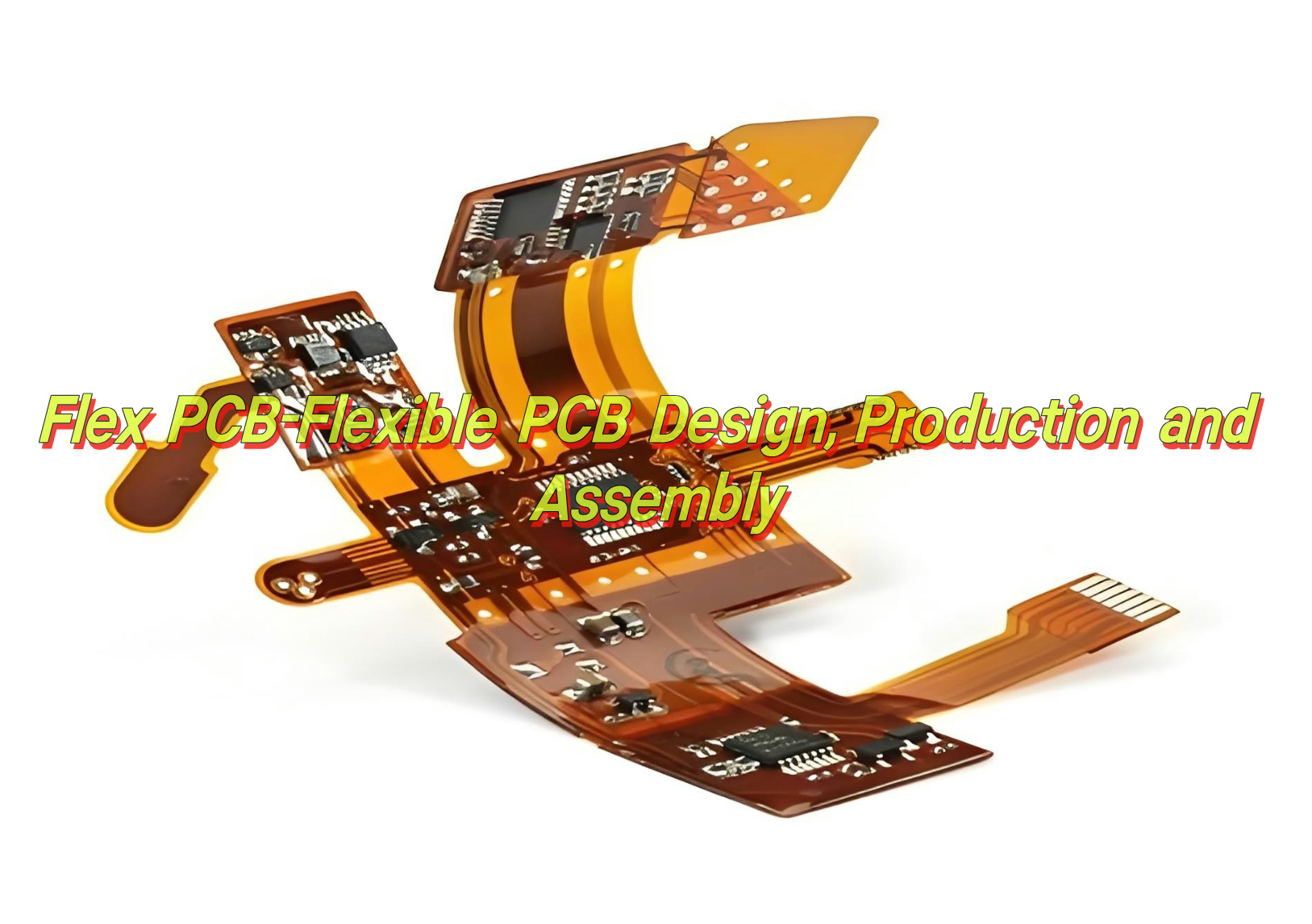
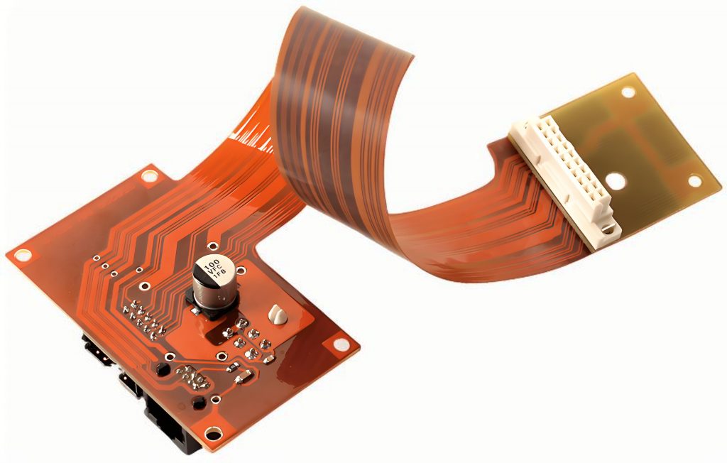
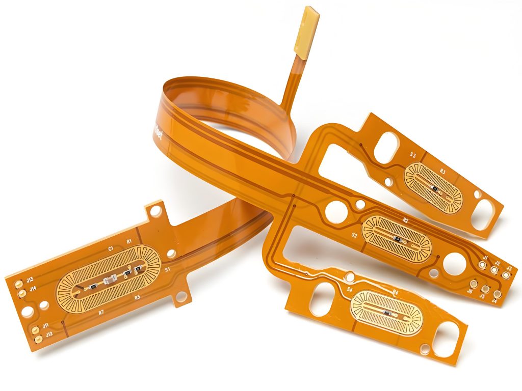
A flex PCB is a printed circuit board made on a flexible substrate instead of the stiff materials used in regular PCBs. Unlike traditional boards, which stay flat, flex PCBs can bend and twist without damaging the copper traces or breaking the substrate. This flexibility gives product designers more freedom to create compact, lightweight, and innovative devices.
Many flexible PCBs use polyimide as the base, which handles heat well and stands up to constant movement. Because they bend without breaking, they are ideal for wearable devices, automotive controls, medical equipment, and any application where space is tight. Plus, flexible PCBs reduce connectors and wiring, lowering the chance of failure points.
Best Technology has over 18 years of experience in flex PCB design, manufacturing and assembly. Our one-stop service helps you simplify your supply chain while improving product reliability. Contact Best Technology at sales@bestpcbs.com today to learn how we support your projects with high-quality flex PCBs, low MOQ, fast delivery and competitive price.
What Are the Components of a Flex PCB?
Flex PCB mainly consists of the following parts:
- Substrate layer
The substrate layer of FPC is usually made of polyimide (PI) or polyester (PET) materials. PI has excellent heat resistance, mechanical strength and electrical insulation, while PET substrate is cheaper, but its heat resistance and chemical resistance are slightly inferior to PI.
- Conductive layer
The conductive layer is mainly composed of copper foil. There are two commonly used copper foils: electrolytic copper foil and rolled copper foil. Electrolytic copper foil has a lower cost and is suitable for applications with low flexibility requirements; while rolled copper foil has good ductility and is suitable for scenarios that require high flexibility and high-frequency bending.
- Coating film layer
The covering film layer is used to protect the copper foil circuit and prevent the influence of the external environment, such as moisture, dust and mechanical damage. The cover film is usually made of the same material as the substrate, such as PI or PET, with a thickness between 0.0125mm and 0.05mm.
- Adhesive layer
The adhesive layer is used to bond the materials of different layers together. Common adhesive materials are acrylic and epoxy resins, which perform well in heat resistance, chemical resistance and flexibility.
- Solder mask
The solder mask is used to protect the soldering area of the circuit, prevent the flow of tin during soldering, and protect the circuit from being short-circuited by solder. The solder mask usually uses green, blue or transparent solder mask ink.
- Surface treatment layer
The surface treatment layer is used to improve the welding performance and reliability of the FPC. Common surface treatments include tin plating and gold plating.
What Are the Components of a Flex PCB?
What Are the Advantages of Flexible PCB?
- Bendability and flexibility
Flexible PCB can bend and fold without affecting the circuit operation, and can adapt to various complex shapes and spatial layouts, which makes it adaptable to various irregular installation requirements.
- Light and thin features
Compared with rigid PCB, flexible PCB is thinner and lighter, which helps to reduce the size and weight of the device and make electronic equipment more portable.
- High reliability
Flexible PCB is not easily affected by vibration and shock, can work stably in harsh environments, and has high reliability.
- High temperature resistance
Flexible PCB can work in high temperature environments and is suitable for electronic equipment in high temperature working environments.
- High production efficiency
The production process of flexible PCB can be completed by robots, which can realize the production of multiple boards at one time, improve production efficiency, and shorten product development cycle.
- Diversified design
Flexible PCB can be customized according to strict physical dimension restrictions to meet the needs of various complex equipment structures.
- High safety
The wires of flexible circuit boards are connected as a whole, which reduces the error problem when the wires are connected and reduces the occurrence of failures.
What Are the Advantages of Flexible PCB?
How Do You Make a Flexible PCB?
The design process of flexible PCB can be divided into the following core steps, combined with key links such as material selection, structural planning and manufacturing process:
1. Demand analysis and planning stage
- Clear functional requirements
Determine the core parameters of the circuit such as functional modules, signal types (high frequency/low frequency), and current carrying capacity as constraints for subsequent design.
- Three-dimensional structure planning
Define the bending area, folding angle and dynamic motion path according to the product space layout to avoid the concentration of lines in the mechanical stress concentration area.
- Layer number and size definition
Select single-layer, double-layer or multi-layer structure according to the complexity of the circuit, and give priority to compact layout to save space.
2. Material selection and structural design
- Substrate selection
Select polyimide (PI) or polyester (PET) substrate according to the application scenario. PI material with stronger temperature resistance is preferred in high temperature environment.
- Conductive layer configuration
Use rolled copper foil to improve bending life. The copper thickness is selected in the range of 18μm-35μm according to the current demand. It is recommended to use ultra-thin copper layer in dynamic bending scenarios.
- Protective layer design
Cover the non-welding area with polyimide cover film, and use reinforcement materials (such as stainless steel sheets) in the dynamic bending area to improve mechanical strength.
3. Circuit design and verification
- Wiring rule setting
The line direction in the bending area is kept perpendicular to the bending direction, and arc corners are used to avoid right-angle routing. Equal-length routing is implemented for key signal lines, and staggered layout is used for adjacent.
- Layer lines to reduce crosstalk
Grid copper plating is used to improve flexibility in the ground layer.
- Impedance control and simulation
Impedance matching calculation is performed on high-speed signal lines, and electromagnetic simulation is performed using tools such as HFSS to verify signal integrity.
- Thermal stress analysis
Use FEA software to simulate the fatigue characteristics of materials after multiple bending, and optimize the routing path and reinforcement scheme.
4. Production file output
- Stack-up drawing
Clearly define the material thickness, adhesive type and cover film window position of each layer, and mark the special process requirements of the dynamic bending area.
- Gerber file generation
Includes circuit layer, drilling diagram, shape cutting diagram, etc. The rigid-flexible board needs to mark the transition structure of the rigid area and the flexible area separately.
- Process description document
Special areas are marked with electroplating requirements (such as selective gold treatment in dynamic bending areas), and the PI cover film window opening accuracy requirements (±0.05mm) are noted.
5. Manufacturability verification
- DFM inspection
Verify key parameters such as minimum line width/line spacing (generally ≥75μm), distance from via to bending area (≥3 times the board thickness), and reinforcement material fitting accuracy.
- Sample test
Perform reliability verification such as dynamic bending test (usually requiring more than 100,000 times without breakage), insulation resistance test under high temperature and high humidity environment, etc.
How to Manufacture Flex PCB Board?
The production process of flexible PCB (FPC) includes the following main steps:
1. Design review
Before prototyping, the design of the flexible PCB needs to be reviewed first. This step mainly checks the rationality, feasibility and potential manufacturing problems of the design. Design review is usually completed by a professional team of engineers, who will carefully evaluate the design documents based on experience and technical specifications.
2. Material preparation
Prepare the corresponding materials according to the requirements of the design documents. The main materials of flexible PCB include conductive materials, insulating materials and substrates. The choice of materials directly affects the performance and quality of flexible PCBs.
3. Production process:
- Graphic production
Coat a layer of dry film photoresist on the copper foil, expose and develop the circuit pattern, and then use an etchant to remove the unnecessary copper, retain the designed circuit part, and form the basic conductive pattern.
- Cover film bonding
Cover the protective film on the line through the lamination process to prevent the circuit from being oxidized or damaged. The cover film needs to be pressed under high temperature and high pressure to ensure good adhesion to the circuit.
- Drilling and electroplating
Drill holes, through holes or mounting holes according to the design drawings. These holes are used for electrical connection between multi-layer FPCs or fixing of components. Hole metallization is to form metal channels through electroplating to ensure the conduction between the upper and lower layers of the circuit.
- Surface treatment
Including gold plating, silver plating, tin plating, etc., select the appropriate treatment process according to the application requirements to improve the corrosion resistance and weldability of the FPC.
- Forming and punching
Punch the FPC according to the specified size according to the designed shape to form the final board shape. This process requires high precision to ensure that the finished product size meets the design requirements.
- Electrical testing
The FPC soft board after forming needs to be tested for electrical performance to ensure that the circuit is well conductive, the insulation meets the standard, and there is no short circuit and open circuit.
- Quality inspection
After completing the production process, the flexible PCB needs to be quality inspected. Mainly check whether the appearance, size, electrical performance and other aspects of the product meet the design requirements. Quality inspection is usually completed by a professional quality inspection team, who will use a variety of advanced testing equipment and methods to conduct strict inspections on the products.
- Packaging and shipment
Flexible PCBs that have passed quality inspection will be packaged and prepared for shipment. The selection of packaging materials and packaging methods need to take into account product protection and safety during transportation.
Flex PCB Manufacturer
Choosing the best flex PCB manufacturer means looking for experience, equipment quality, and customer support. Flex PCB production requires specialized machinery and careful handling at every step, so a factory with proven experience matters.
A good manufacturer offers design advice to help avoid costly errors. They also provide fast prototyping so design changes can be tested quickly before moving to full production. Beyond production, reliable after-sales support helps catch any issues during assembly at your facility.
Best Technology offer full-service capabilities, including flex PCB design, prototyping, production, and assembly. This simplifies communication and reduces the chance of errors caused by working with multiple suppliers. A trusted manufacturer also keeps materials in stock, shortening lead times and helping you stay on schedule.
What Is Rigid PCB vs Flex PCB?
The main differences between rigid PCB and flexible PCB are in terms of substrate, structure, application field, stress resistance, cost, design requirements and maintainability.
- Substrate
Rigid PCB: FR-4 (glass fiber reinforced epoxy board) is usually used as the substrate, which has high mechanical strength and stable electrical performance.
Flexible PCB: The substrate is mostly polymer materials such as polyimide (PI) or polyester (PET), which has good flexibility and lightness.
- Structure
Rigid PCB: It usually has a multi-layer structure, consisting of multiple layers of substrate and conductive layer, suitable for applications requiring high mechanical strength and stable electrical performance.
Flexible PCB: It is usually a single-layer or double-layer structure with a thin thickness, which is more suitable for miniaturized and lightweight product design.
- Application
Rigid PCB: It is widely used in computers, communication equipment, household appliances and other fields that require high strength and stable performance.
Flexible PCB: Mainly used in flexible displays, wearable devices, smartphones and other fields that require flexibility and compact design.
- Stress resistance
Rigid PCB: With high stress resistance, suitable for bearing large mechanical pressure and thermal stress.
Flexible PCB: Although the stress resistance is relatively low, it has good adaptability to bending and folding stress.
- Cost
Rigid PCB: The production cost is relatively low, and the raw materials and production process are relatively mature.
Flexible PCB: Due to the special substrate and production process, the production cost is relatively high.
- Design requirements
Rigid PCB: The design is relatively simple, and the wiring space and installation method requirements are relatively low.
Flexible PCB: The design needs to consider factors such as wiring space, bending radius, and folding times, and the design is more difficult.
Where are flexible PCBs used?
Flexible PCB (Flexible Printed Circuit Board, FPC) has a wide range of applications, mainly including the following aspects:
- Smartphones and smart watches
Flexible PCB is widely used in smartphones and smart watches with its light and flexible characteristics. It can adapt to complex internal structures and provide stable electrical performance.
- Automotive electronics
In the field of automotive electronics, flexible PCB is used for in-vehicle entertainment systems, sensors and control systems, etc., providing lightweight and high-reliability solutions.
- Medical devices
Flexible PCB also has important applications in medical devices, such as endoscopes and catheters, which can adapt to complex in vivo environments and provide high reliability and flexibility.
- Aerospace
In the field of aerospace, flexible PCB is used in satellite communication systems, navigation and control systems, power and energy management systems, etc., to meet the high reliability, lightweight and high-density integration requirements in extreme environments.
- Consumer electronics
Flexible PCB is also widely used in the field of consumer electronics, such as wearable devices, tablets and laptops, providing miniaturized and high-density installation design requirements.
Conclusion
Flex PCBs give product designers the freedom to create smaller, lighter, and more reliable products across many industries. Whether you need a simple flex PCB design for a wearable or a complex multi-layer flexible board for medical equipment, understanding the process helps you make better choices.