
What is a Wi-Fi Antenna PCB?
A Wi-Fi antenna PCB is a specialized printed circuit board used in the design and functionality of wireless communication devices. It serves as the base on which a Wi-Fi antenna is integrated, enabling seamless wireless communication. These PCBs are crucial components for devices that rely on Wi-Fi signals, from smartphones to routers. The antenna is embedded into the PCB, ensuring optimal signal transmission and reception. Without a high-quality antenna PCB, the Wi-Fi signal may experience disruptions, leading to slower connections or weaker signals.
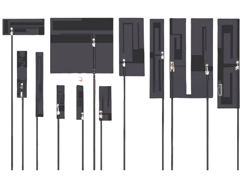
Types of Wi-Fi Antenna PCBs
Wi-Fi antenna PCBs come in different types, each tailored to specific needs and designs. Here are some of the most common types:
- Monopole Antenna PCBs
A monopole antenna is a simple design with one main conductor, typically a straight wire. This type is cost-effective and efficient for most consumer-grade devices. It is often used in compact devices where space is limited.
- Dipole Antenna PCBs
The dipole antenna consists of two conductors and is often used for higher-performance applications. It offers better radiation patterns and is ideal for devices that require broader coverage.
- Patch Antenna PCBs
A patch antenna is a popular choice for Wi-Fi applications due to its compact design and high efficiency. It can be integrated into devices with minimal space and offers good directional performance.
- Helical Antenna PCBs
Helical antennas are used when a circular or omnidirectional signal is required. These are highly effective in applications like Wi-Fi routers or mobile devices that need signals in all directions.
- Array Antenna PCBs
Arrays combine multiple antennas to improve signal strength and coverage. They are often used in complex communication systems where range and reliability are crucial.
Advantages of Wi-Fi Antenna PCBs
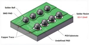
Wifi PCB antenna is printed wires on the PCB board to achieve signal radiation and reception. Common PCB antenna designs include straight, F-shaped, serpentine or circular lines, and the length is usually a quarter wavelength to ensure the best signal transmission efficiency.
- Cost effectiveness: PCB antennas are generally less costly as they do not need to be assembled separately and can be integrated directly on the motherboard, simplifying the production process and reducing costs.
- Space efficiency: PCB antenna is built-in, takes up less space, suitable for space limited equipment, such as smart wearable devices and drones.
- Easy integration: PCB antenna can be printed directly on the circuit board, simplifying the assembly process, making the whole machine assembly more convenient.
- Stability: PCB antennas reduce external components, reduce the risk of damage, and are less susceptible to physical damage.
- Wi-Fi Antenna PCB PCB antenna design can be optimized at the design stage to adapt to different design needs and shapes.
What is the Best Material for Wi-Fi Antenna?
The material used in the Wi-Fi antenna PCB plays a significant role in its performance. The best material for Wi-Fi antenna PCBs ensures low signal loss, high efficiency, and overall durability. Here are some materials commonly used for Wi-Fi antenna PCBs:
- FR4
FR4 is one of the most common PCB materials. It offers a good balance between cost and performance. While it may not be ideal for high-frequency applications, it’s suitable for most consumer-grade devices.
- Rogers RT/duroid
Rogers materials like RT/duroid are widely used for high-performance antenna designs. They provide excellent dielectric properties, making them ideal for high-frequency signals like Wi-Fi.
- Ceramic PCBs
Ceramic-based PCBs are used in applications requiring extremely low loss and high thermal conductivity. They are suitable for high-frequency Wi-Fi applications.
- Polyimide
This material is used in high-temperature environments due to its excellent thermal stability. Polyimide is often used for flexible PCBs in compact and portable Wi-Fi devices.
Wi-Fi PCB Antenna Design Considerations
Designing a Wi-Fi PCB antenna requires careful planning to ensure optimal performance, minimal signal interference, and reliable wireless connectivity. Here are key factors to consider:
1. Antenna Selection and Structural Requirements
- For optimal performance, prioritize the PIFA antenna (Planar Inverted-F Antenna) over standard chip antennas, as it offers higher success rates and better efficiency. Ensure the antenna length corresponds to a quarter of the free-space wavelength (e.g., approximately 30.6mm for 2.4GHz).
- If using SMT chip antennas or FPC antennas, reserve the required pad size (e.g., 2×3mm) and maintain a copper-free clearance of at least 0.8mm around them. On-board PCB antennas are suitable for cost-sensitive applications, but meandered traces should be used to optimize space utilization.
2. Layout and Routing Guidelines
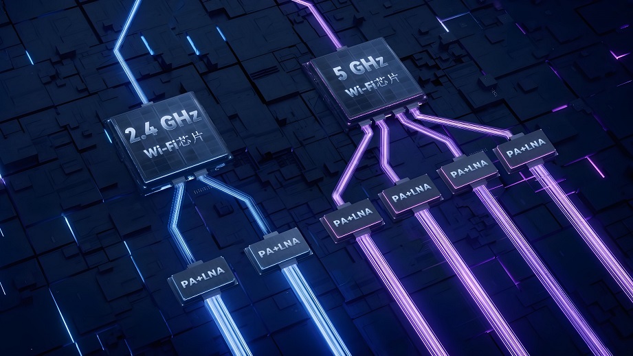
- RF traces should maintain 50Ω impedance matching, preferably using microstrip lines, and avoid vias. A continuous ground plane should be placed beneath the RF trace.
- The antenna must be kept away from metal objects (≥15mm) to prevent interference. Avoid metal-coated enclosures or fully sealed metal structures that could block signals.
- The RF module should be positioned close to the antenna to shorten the transmission path while keeping a safe distance from high-speed signals (e.g., Class-D amplifiers and audio circuits).
3. Grounding and Clearance Design
- A continuous ground plane beneath the antenna is required, ideally with a length equal to the antenna itself (e.g., 30.6mm for 2.4GHz). If space is limited, grounding through the bottom layer can be considered.
- The antenna area must remain clear of components and other traces, with a copper-free clearance of at least 0.8mm around it.
4. Interference Mitigation
- Metal structures (e.g., enclosures) should be properly grounded at multiple points to prevent poor grounding, which could lead to signal reflection and reduced efficiency.
- Differential signal traces (e.g., audio signals) should be routed as parallel and equal-length pairs and kept away from RF areas.
5. Performance Optimization
- Use simulation tools to fine-tune antenna parameters (e.g., height, meandered trace spacing) to ensure bandwidth and gain match Wi-Fi frequency requirements.
- External antennas (e.g., dipole or FPC antennas) can improve gain but should be evaluated for installation space and enclosure material compatibility.
Wi-Fi PCB Antenna Applications
- Smartphones and Tablets – These devices rely heavily on Wi-Fi antennas for high-speed internet access. Wi-Fi antenna PCBs ensure stable connectivity, even in crowded environments.
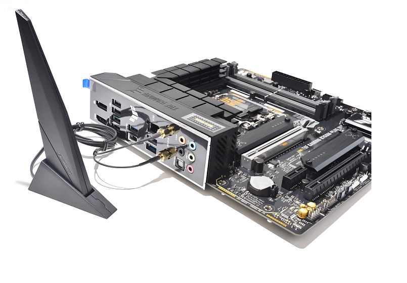
- Routers and Modems – Wi-Fi routers and modems use high-performance antenna PCBs to provide strong, consistent signals throughout a home or office.
- IoT Devices – As the Internet of Things (IoT) continues to grow, Wi-Fi antenna PCBs are integral to the communication capabilities of connected devices, including smart home products.
- Wearable Devices – Many wearables like smartwatches require compact Wi-Fi antenna PCBs for wireless communication, ensuring a seamless user experience.
- Consumer Electronics – Various consumer electronics, from TVs to game consoles, integrate Wi-Fi antenna PCBs for internet connectivity and streaming capabilities.
Turn-Key Wi-Fi Antenna PCB Manufacturer
Best Technology is a leading PCB manufacturer with over 18 years of experience in the industry. We specialize in designing and producing high-quality Wi-Fi antenna PCBs for various applications, including consumer electronics, IoT devices, and industrial communication systems. We offer turn-key manufacturer handles the entire process, from design to assembly, offering a seamless experience.
With a strong commitment to quality, we follow rigorous testing procedures and use only the best materials, such as Rogers and ceramic PCBs, to enhance antenna performance. Whether you need a standard or custom Wi-Fi antenna PCB, Best Technology provides expert solutions tailored to your specific needs.
If you’re looking for a reliable manufacturer that delivers precision, durability, and superior signal quality, Best Technology is your trusted partner. Contact us today to discuss your Wi-Fi antenna PCB requirements!
FAQs
1. What is the difference between a Wi-Fi PCB antenna and a traditional external antenna?
Wi-Fi PCB antennas are integrated into the circuit board, offering a more compact design. Traditional external antennas are often bulkier and may be prone to damage.
2. Can I use a Wi-Fi antenna PCB for other wireless communication systems?
Yes, Wi-Fi antenna PCBs can be adapted for other wireless communication standards, such as Bluetooth or Zigbee, by adjusting the design to match the required frequencies.
3. How can I improve the performance of my Wi-Fi antenna PCB?
Optimizing the layout, material choice, and impedance matching can help improve the performance of your Wi-Fi antenna PCB.
4. Is it possible to manufacture custom Wi-Fi antenna PCBs?
Yes, many PCB manufacturers offer custom designs based on your specific needs, whether it’s for unique form factors or enhanced performance.
You may also like


Tags: wifi antenna pcb, wifi antenna pcb design, wifi antenna pcb manufacturer