pcb
Home > Blog

Archive for the ‘Design Guide’ Category

Which Controller Should I Use For UAV?
Wednesday, November 27th, 2024

Choosing the right controller for a UAV depends on various factors like the type of UAV, its purpose, your experience level, and budget.

  • Purpose: If you use drones for professional missions, you may need a powerful GCS. For temporary flights, a radio controller may be sufficient.
  • Budget: If you’re on a tight budget, a pocket radio may be the best option.
  • Drones: Top drones are usually equipped with good controllers, so you may not need to buy a separate remote.
Which Controller Should I Use For UAV?

Popular Flight Controllers for UAVs

  • DJI Flight Controllers (e.g., A3, N3): Great for commercial applications, high stability, and ease of use.
  • Pixhawk (Cube Orange, PX4): Open-source, highly customizable, and suitable for research and commercial use.
  • BetaFlight Controllers: Excellent for racing drones and hobbyists.
  • Navio2: Turns a Raspberry Pi into a flight controller, ideal for custom applications and experimentation.

What Is a UAV Flight Controller?

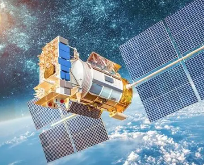
UAV is the abbreviation of Unmanned Aerial Vehicle, is the use of radio remote control equipment and self-provided program control device unmanned aircraft, including unmanned helicopter, fixed wing aircraft, multi-rotor aircraft, unmanned airship, unmanned umbrella aircraft. In a broad sense, it also includes near-space vehicles (20-100 km airspace), such as stratospheric airships, high-altitude balloons, and solar-powered drones. From a certain point of view, drones can complete complex air flight tasks and various load tasks under unmanned conditions, and can be seen as “air robots”.

The flight control system is the core system of the UAV to complete the whole flight process such as take-off, flight, task execution and return recovery. Flight control is equivalent to the role of the pilot to the man-machine of the UAV, and we believe that it is one of the most core technologies of the UAV. Flight control generally includes three parts: sensor, on-board computer and servo actuation equipment, and the functions achieved mainly include UAV attitude stabilization and control, UAV mission equipment management and emergency control.

Which Controller Should I Use For UAV?

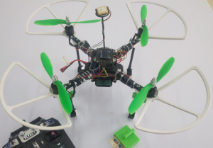
Which Controller Is Used in a Drone?

Two types of controllers are integral to drone operations: the flight controller and the remote controller. The flight controller is mounted on the drone and manages its internal systems. It monitors data from sensors like gyroscopes, accelerometers, and barometers to maintain stability. Additionally, it processes inputs from the pilot, ensuring precise execution of commands.

The remote controller is what the pilot uses to steer the drone. It communicates wirelessly with the flight controller, usually via radio frequencies. Modern remote controllers come equipped with ergonomic designs, customizable buttons, and live feed displays.

For example, DJI drones use advanced proprietary systems, combining high-performance flight controllers with intuitive remotes. Racing drones, on the other hand, often rely on lightweight controllers designed for speed and agility.

Does the Military Use Xbox Controllers for Drones?

Yes, the military sometimes uses Xbox controllers for drones. This might seem unconventional, but it has practical benefits. Xbox controllers are widely recognized and easy to operate. Many soldiers are already familiar with their layout from gaming, which reduces training time.

For less critical missions, adapting Xbox controllers is cost-effective. They provide a user-friendly interface for operating UAVs without compromising functionality. However, for advanced military drones, specialized controllers with enhanced security and precision are standard. These controllers can handle encrypted communication, complex tasks, and long-range operations.

While the use of Xbox controllers highlights creativity, it’s limited to specific scenarios. For professional-grade UAVs, more robust systems remain the norm.

Can You Use Different Controllers for Drones?

Can you use different controllers for drones? Yes, you can use different controllers for drones, but it requires careful planning. Most drones come with a default remote, but advanced users often switch to alternatives for better functionality. For example, a racing drone enthusiast might replace the stock controller with one offering lower latency and faster response.

Which Controller Should I Use For UAV?

Compatibility is crucial when using a different controller. The new remote must support the communication protocol of the drone’s flight controller. Common protocols include SBUS, PPM, and DSMX. Mismatched systems can result in loss of control or limited functionality.

Some controllers allow users to connect their smartphones or tablets for enhanced capabilities. This is popular with photography drones, where touchscreens can display live video feeds or advanced settings. When experimenting with new controllers, always test the setup in a safe environment.

Which Flight Controller Is Used in DJI?

DJI is a leader in the UAV industry, known for its advanced flight controllers. Popular models include the Naza, A3, and the newer Zenmuse H20 series. These controllers are packed with features tailored for seamless performance:

  • Stability: DJI controllers use GPS and IMUs (Inertial Measurement Units) to maintain precise positioning.
  • Automation: Intelligent flight modes like waypoint navigation, orbit mode, and follow-me functions are common.
  • Integration: DJI’s controllers work seamlessly with their proprietary motors, cameras, and software.

Can a Drone Fly Without a Flight Controller?

No, a flight controller is essential for flying a drone. It processes inputs, balances the drone, and manages its systems. Without a flight controller, the UAV cannot interpret pilot commands or stabilize itself.

Even basic drones rely on flight controllers for manual control. Advanced models use them for automation and sensor integration. Attempting to fly without one would result in erratic movements and likely crashes.

What Is the Best Flight Controller for 2024?

Choosing the best flight controller in 2024 depends on your needs. Here are some top contenders based on performance and features:

  • Pixhawk 6X:

A favorite among hobbyists and professionals. It supports advanced automation and is compatible with Ardupilot firmware.

  • DJI A3 Pro:

Designed for high-end commercial drones, this controller excels in stability and precision.
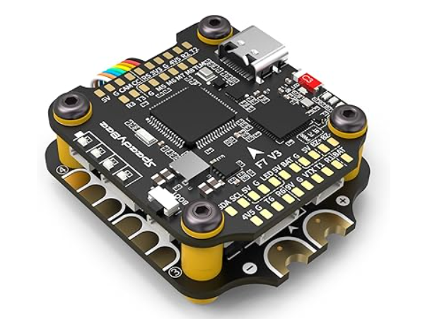
  • Betaflight F7:

A top choice for racing drones, known for low latency and fast response.

  • CubePilot Orange:

Ideal for industrial applications, this controller handles heavy payloads and complex missions.

  • Holybro Kakute F7:

Affordable yet reliable, it suits beginners venturing into custom builds.

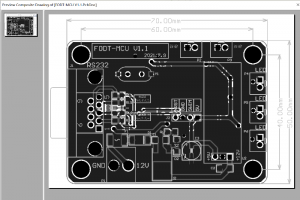
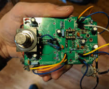
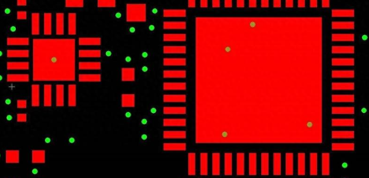
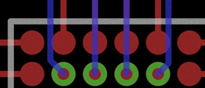
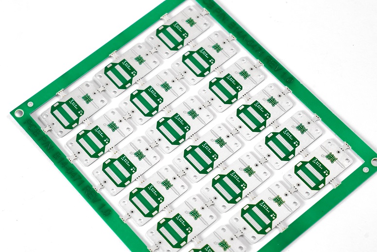
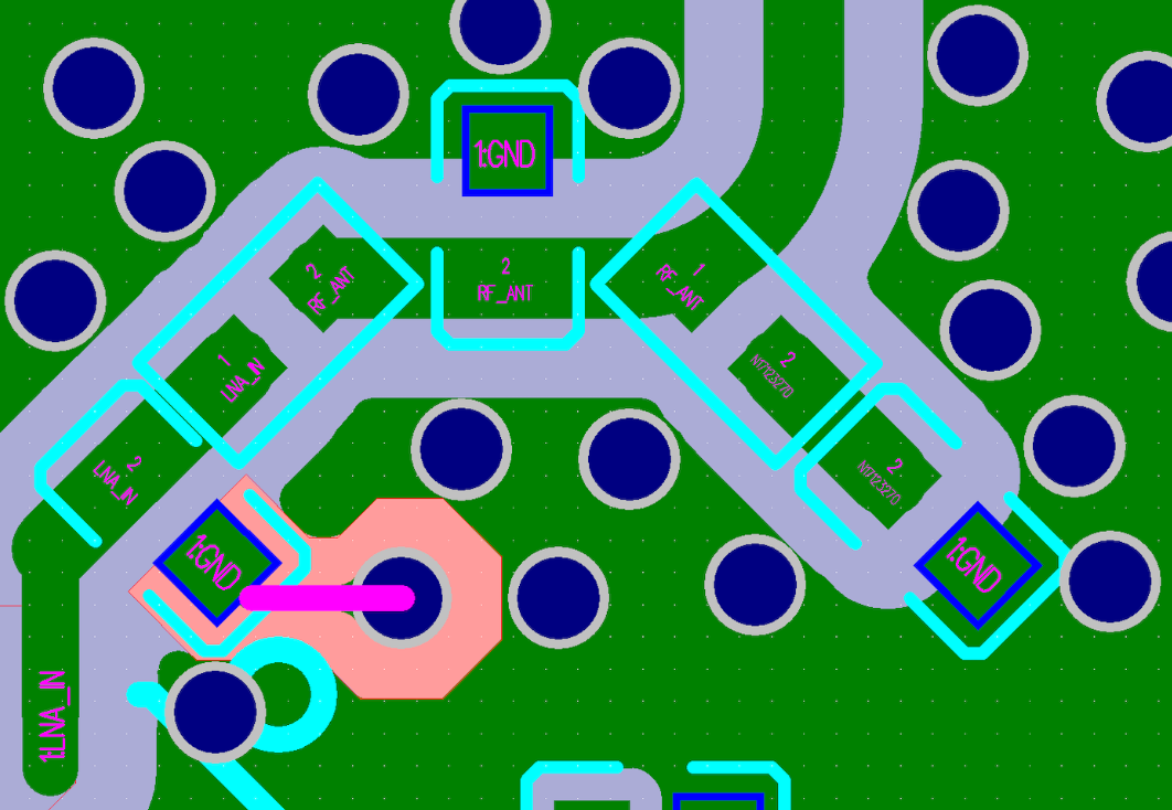
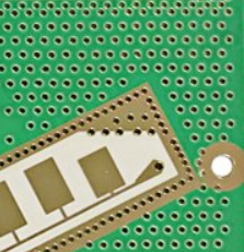
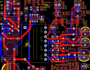
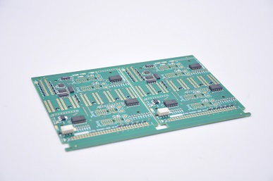
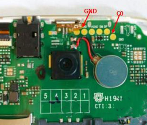
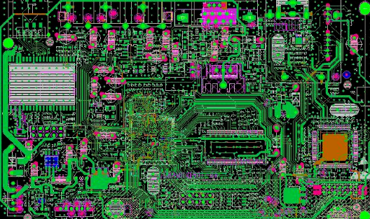
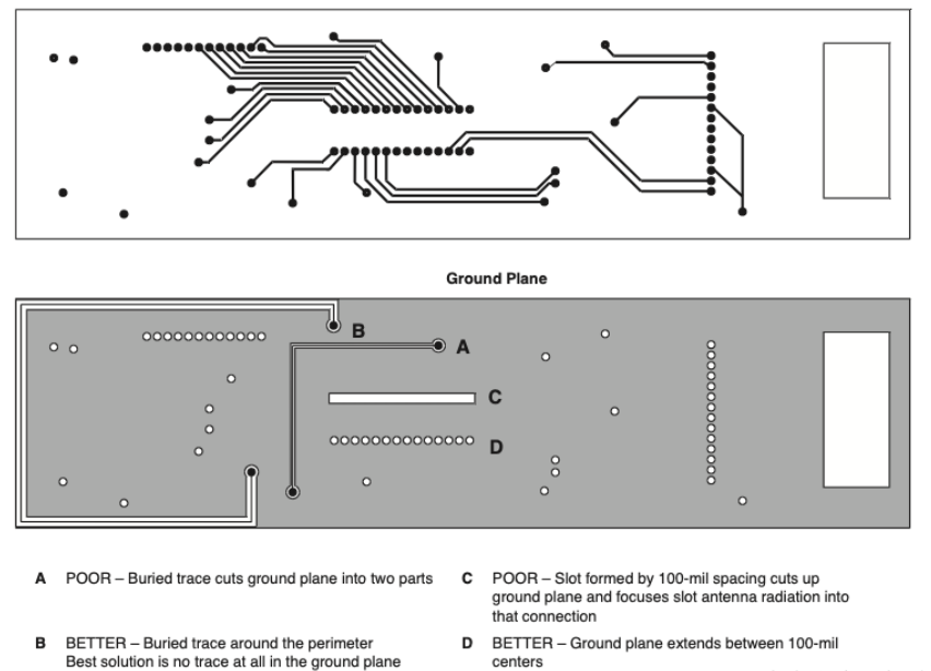
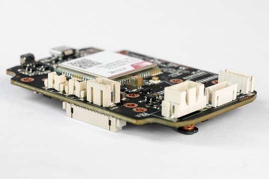
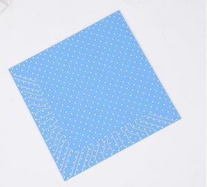
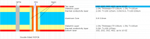
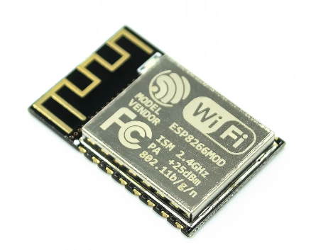
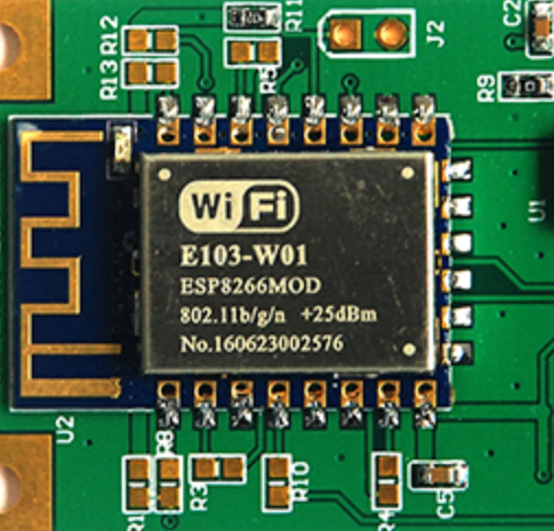
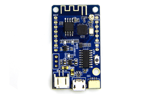
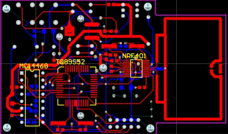
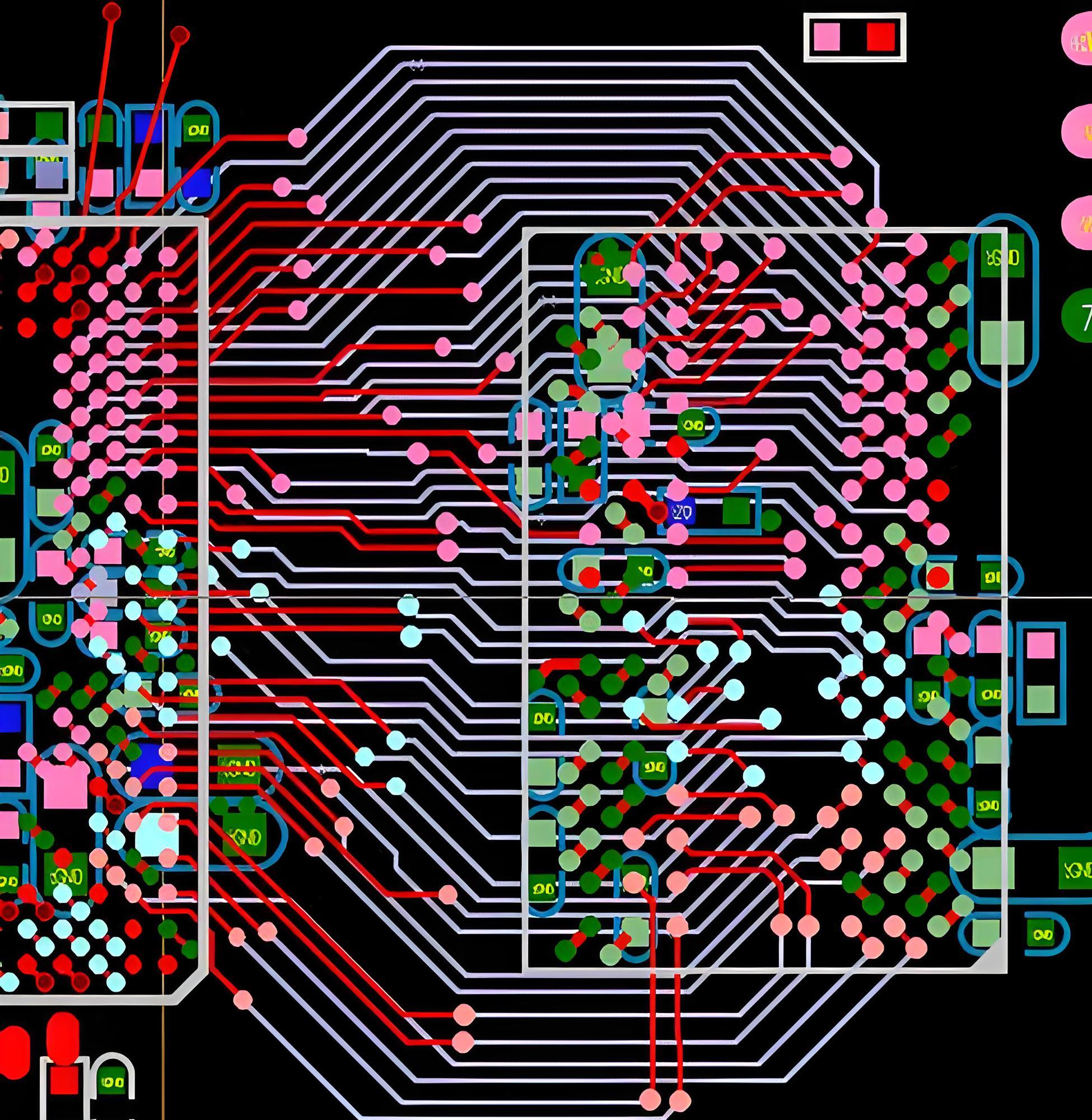
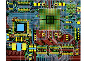
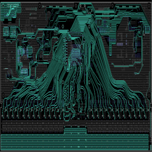
Key Element in a UAV Controller: Drone Circuit Board

The drone circuit board is the backbone of the UAV controller. It houses essential components that govern the drone’s functions, from navigation to communication. Without this intricate board, a drone would lack the ability to process commands or execute movements effectively.

Best Technology made various drone circuit boards for our customers, we offer one-stop service from pcb design to PCB manufacturing, aiming to give you a best experience. Interested in it? Contact us right now!

You may also like

Via in Pad Design Guideline & FAQs
Tuesday, November 26th, 2024

What is Via in Pad?

With the improvement of the integration of electronic products, the package of components is getting smaller and smaller, and the pin spacing is also getting smaller and smaller. In complex PCB design, the signal cannot be fanned out without punching the disc hole, and the signal must be drawn from the next layer through the disc hole. Especially in the miniaturization applications of ‌BGA (Ball Grid Array) and ‌SMD (Surface Mount Device) chips, the process of disc holes has been widely used.

Via in pad is a design methodology in PCB manufacturing where vias are directly embedded in the pads of surface-mount devices (SMDs). Traditional vias are placed near the components with traces connecting them to the pads. However, in via-in-pad designs, the vias and pads are combined, which saves space and shortens trace lengths. This approach is particularly useful in HDI PCBs, where board real estate is limited, and signal integrity is critical.

Via in Pad Design Guideline & FAQs

What is Via-in-Pad Plating?

Via-in-pad plating refers to a specialized manufacturing process where vias embedded in pads are filled and plated over to form a smooth, conductive surface. This process involves:

  1. Via Filling: The via hole is filled with a material, often epoxy or a conductive paste, to eliminate voids and provide structural stability.
  2. Copper Plating: The filled via is then plated with copper to create a uniform and conductive layer.
  3. Surface Finish: A finish such as ENIG (Electroless Nickel Immersion Gold) or HASL (Hot Air Solder Leveling) is applied to ensure solderability.

Proper via-in-pad plating prevents solder wicking, a phenomenon where solder flows into the via during reflow, causing insufficient solder on the component leads.

Is Via-in-Pad Expensive?

Via-in-pad designs are undeniably more expensive than traditional vias. The additional manufacturing steps, such as via filling, plating, and the need for precise alignment, contribute to the higher costs. Moreover, the advanced equipment and materials required for this process add to the overall expense.

However, for designs that demand high performance, such as smartphones, medical devices, and aerospace electronics, the benefits of via in pad often outweigh the cost. It allows for compact layouts, improved performance, and better thermal management, making it indispensable for cutting-edge applications.

What Size is a Via-in-Pad?

The size of a via-in-pad is influenced by the PCB’s application, layer count, and the size of the components used. In HDI PCBs, via sizes typically range from 0.15 mm to 0.4 mm in diameter. Microvias, often used in via-in-pad designs, can be as small as 0.1 mm.

The diameter must align with the pad size to avoid compromising the pad’s mechanical and electrical integrity. Designers also need to consider the PCB manufacturer’s capabilities when selecting via sizes, as extremely small vias may require advanced fabrication techniques.

What are the Drawbacks of Via in Pad?

While via in pad offers several advantages, it also comes with notable challenges:

  • Higher cost
  • Soldering defects
  • Complex manufacturing
  • Thermal stress risks
  • Complex manufacturing process

Can You Put Vias Under Components?

Yes, placing vias under components is common in advanced PCB designs, particularly with via in pad. This technique is often used for BGAs, QFNs, and other fine-pitch components.

However, proper design and manufacturing practices must be followed to prevent defects. Filling and plating the vias ensure they do not interfere with soldering. Additionally, simulations and testing are essential to validate the design and ensure reliability.

Traditional Vias vs. Via-in-Pad Design

Traditional vias are placed outside the component pad, with traces connecting them to the pads. While this approach is cost-effective, it consumes more space and may result in longer trace lengths, increasing parasitic effects.

Via in Pad Design Guideline & FAQs

Via-in-pad designs embed the vias directly within the component pads, reducing trace lengths and optimizing space. They enhance signal integrity, thermal performance, and overall board aesthetics but at a higher cost and complexity.

When to Use Via-in-Pad Design?

Via-in-pad designs are not always necessary, but they are indispensable in specific scenarios where performance, space optimization, and thermal management are critical. Below are the situations where via-in-pad designs are most appropriate:

1. High-Density Interconnect (HDI) PCBs

When designing HDI PCBs with compact layouts and high layer counts, via-in-pad is essential. This design technique optimizes the limited space available, allowing for more components and connections on the board. It is particularly useful for devices like smartphones, wearables, and IoT devices where miniaturization is key.

2. Fine-Pitch Components

Via-in-pad designs are commonly used for components with fine pitches, such as:

  • BGA chips: BGAs have numerous pins closely spaced, leaving minimal room for traditional routing. Via in pad provides a clean solution to connect signals directly.
  • QFNs: QFNs require vias under the pads for effective routing and thermal management.
Via in Pad Design Guideline & FAQs

3. High-Speed and RF Applications

In high-speed and RF circuits, signal integrity is paramount. Via-in-pad designs minimize trace lengths, reducing parasitic inductance and impedance mismatches. This makes them ideal for applications like:

  • 5G communication systems
  • High-frequency radar systems
  • Advanced networking equipment

4. Improved Thermal Management Needs

For power components or heat-sensitive devices, via in pad aids in efficient thermal dissipation. By directly connecting the pads to thermal vias leading to internal or external layers, heat is transferred away from the components. This is critical for:

  • High-power LEDs
  • Voltage regulators
  • Power amplifiers

5. Limited PCB Real Estate

In designs with severe space constraints, via in pad maximizes usable board area. This allows for additional routing space and supports high component density without sacrificing performance. Applications like medical implants and aerospace electronics greatly benefit from this approach.

6. Double-Sided Component Placement

When components are placed on both sides of the PCB, traditional vias can interfere with the routing on the opposite side. Via in pad eliminates this issue by embedding the vias within the pads, simplifying double-sided designs.

7. High-Performance Computing Systems

For processors, GPUs, and other high-speed ICs, via in pad ensures reliable power delivery and signal integrity. It is frequently used in:

  • Data centers
  • High-performance workstations
  • AI hardware

Guidelines for Via-in-Pad Design

Via-in-pad designs require meticulous attention to detail to ensure reliability and performance.

1. Decide on the most suitable via type based on your design requirements:

  • Microvias: Ideal for high-density designs due to their small size.
  • Blind/Buried Vias: Useful for connecting internal layers without penetrating through the entire board.
  • Through-Hole Vias: Less common in via-in-pad but may be necessary for specific designs.

2. Fill the vias with appropriate materials to ensure mechanical stability and prevent solder wicking:

  • Non-Conductive Epoxy Fill: Provides a reliable, flat surface for soldering.
  • Conductive Fill: Used when electrical connectivity through the via is needed.

3. The plating over the filled vias should be smooth and flat to avoid soldering issues. Use a high-quality copper plating process to enhance electrical and thermal conductivity.

4. Collaborate with your PCB manufacturer early in the design process to align on their capabilities. This includes:

  • Minimum via diameter and pad size.
  • Spacing requirements between vias and traces.
  • Maximum number of vias that can be placed in pads.
Via in Pad Design Guideline & FAQs

5. Ensure the via size is proportionate to the pad size. A via that is too large can compromise the pad’s structural and electrical integrity, while a too-small via may not provide the necessary connectivity or thermal performance.

6. For high-power applications, incorporate thermal relief patterns or thermal vias.

7. Maintain sufficient spacing between vias and other components or traces to prevent electrical interference or thermal stress.

8. To avoid solder flowing into the via during reflow soldering:

  • Use filled and capped vias.
  • Employ surface finishes like ENIG (Electroless Nickel Immersion Gold) or OSP (Organic Solderability Preservative) for enhanced soldering reliability.

9. When using via in pad for power components or ground connections, thermal relief patterns help prevent excessive heat buildup. These are especially important in high-current designs.

Need assistance in designing via-in-pads in your PCB design? Leave your comments on below, our design experts will help to solve them.

You may also like

RF Board | RF Printed Circuit Board Design Guide
Saturday, November 23rd, 2024

What Are RF Boards?

RF boards, or radio frequency printed circuit boards. RF boards are designed to operate with high-frequency signals, typically within the range of 3 kHz to 300 GHz. This capability makes them a critical component in devices that rely on wireless communication, such as mobile phones, satellite systems, and radar equipment.

Unlike regular FR4 PCBs, RF boards are optimized to handle electromagnetic waves in the radio frequency range. They use specialized materials and designs to minimize signal loss, avoid interference, and maintain stable operation. Their importance continues to grow with advancements in wireless technologies, the Internet of Things (IoT), and 5G networks.

The design and manufacturing of RF boards demand meticulous attention to detail, as even minor issues can significantly impact their performance. These boards are vital for applications where precision and reliability are non-negotiable.

RF Board | RF Printed Circuit Board Design Guide

Advantages of RF Boards

  1. High-frequency systems require consistent and stable signal transmission. RF boards are designed to reduce signal distortion and ensure accuracy, even in complex environments.
  2. The specialized materials used in RF boards, such as PTFE and Rogers laminates, have low dielectric constants.
  3. RF boards are built to handle heat efficiently.
  4. RF boards can be tailored to meet specific requirements, including frequency range, size, and power capacity.
  5. With RF boards, engineers can integrate cutting-edge technologies like 5G, IoT, and advanced radar systems.
  6. RF boards design ensures long-term reliability, even under challenging conditions.

What Is the Difference Between RF PCB and Normal PCB?

While standard PCBs and RF PCBs may appear similar at first glance, their functions, materials, and design considerations set them apart.

  • Frequency Handling

Standard PCBs are designed for low to medium frequencies and do not require the precision needed for high-frequency signals. RF PCBs, on the other hand, are built to handle frequencies ranging from kilohertz to gigahertz.

  • Material Properties

Materials are a defining factor. Normal PCBs commonly use FR-4, a cost-effective and versatile material. In contrast, RF boards use materials like PTFE, Rogers laminates, or ceramic substrates. These materials have low dielectric constants and low loss tangents, ensuring minimal signal degradation.

  • Signal Integrity

RF boards are engineered to minimize crosstalk and interference. Design considerations include impedance matching and controlled trace dimensions, which are not as critical in standard PCBs.

  • Application Areas

While standard PCBs are widely used in consumer electronics, RF PCBs find their place in specialized fields like telecommunications, aerospace, and medical devices, where high-frequency signals are essential.

Which Material Is Commonly Used for RF PCBs?

Material selection is critical when designing RF boards. The right material ensures that the board can handle high-frequency signals with minimal loss and distortion.

  • PTFE (Polytetrafluoroethylene)

PTFE is a common choice for RF PCBs due to its excellent electrical properties. It has a low dielectric constant, which supports stable signal propagation. PTFE is also resistant to heat, making it suitable for high-power applications.

  • Rogers Laminates

Rogers laminates are widely used in RF designs. These materials offer exceptional thermal stability and low loss tangents, ensuring reliable performance. They are also easy to process, making them a favorite among manufacturers.

  • Ceramic-Filled Substrates

For applications requiring high power and thermal management, ceramic-filled substrates are an excellent option.

  • Liquid Crystal Polymer (LCP)

LCP is a flexible, lightweight material suitable for RF boards used in compact devices like smartphones and wearables.

  • Hybrid Materials

Some RF PCBs combine multiple materials to balance cost, performance, and manufacturability. Hybrid materials allow designers to meet specific application requirements effectively.

What Are RF Circuits Used For?

Telecommunication Systems – RF circuits are the backbone of mobile networks, Wi-Fi routers, and wireless communication devices.

Aerospace and Defense – Radar systems, satellite communication, and military-grade navigation rely on RF circuits.

IoT Devices – The Internet of Things depends heavily on RF circuits for connectivity. From smart home systems to industrial sensors, these circuits enable real-time data exchange.

Medical Equipment – In healthcare, RF circuits support technologies like MRI machines and wireless patient monitoring systems.

Automotive Applications – RF circuits play a key role in modern vehicles, powering advanced driver-assistance systems (ADAS), vehicle-to-everything (V2X) communication, and keyless entry systems.

RF PCB Design Guidelines

Designing RF PCBs can be as challenging as addressing electromagnetic interference (EMI). Success often requires careful planning and attention to the following aspects:

1. Transmission Lines

  • Select the correct transmission line type (microstrip or stripline) based on the required 50Ί characteristic impedance.
  • Use impedance calculation tools to design consistent impedance lines and determine appropriate line width and spacing.
  • Ensure continuity in RF transmission lines by maintaining uniform widths and spacing.
  • Avoid abrupt transitions or splits in RF signal paths as they impact impedance.
  • Provide a clean ground reference under the transmission line without interference from other signals.
  • Minimize transmission line lengths to reduce signal loss, and use wider traces for power lines.
  • Use compensated bends for corners, avoiding sharp angles.
  • Avoid forks, stubs, or parallel placement of other lines near RF transmission lines.
  • Refrain from placing test points directly on RF transmission lines.
RF Board | RF Printed Circuit Board Design Guide

2. PCB Layer Stacking

  • A recommended four-layer stackup for RF PCBs includes:

Top Layer: RF ICs, components, transmission lines, decoupling capacitors, and antennas.

Layer 2: Ground plane.

Layer 3: Power plane.

Bottom Layer: Non-RF components and signal traces.

  • Ensure a complete and continuous ground plane for RF signal integrity.
  • Follow the “20H rule,” where the power plane edges are recessed by at least 20 times the plane-to-plane spacing to reduce EMI.

3. Power Decoupling

  • Place decoupling capacitors as close to power pins as possible.
  • Use a combination of large and small capacitors for filtering different noise frequencies.
  • Keep decoupling capacitors and power layers on the same plane, prioritizing smaller values near IC pins.
  • Avoid vias between decoupling capacitors and IC power pins.
  • Each decoupling capacitor should have a dedicated ground via.

4. Vias

  • Use multiple vias to connect layers, spaced no greater than Îť/20.
  • Place ground vias near signal vias to minimize parasitics.
  • Avoid sharing vias between solder pads and signal traces.
  • Prefer smaller vias for reduced parasitic effects but balance against manufacturing costs.
  • Employ ground vias around sensitive components to enhance EMC shielding.
RF Board | RF Printed Circuit Board Design Guide

5. Capacitors

  • Use C0G/NP0 capacitors for temperature stability and frequency consistency.
  • For decoupling, select capacitors with self-resonant frequencies (SRF) near the operational range.
  • Employ smaller packages (e.g., 0201 or 0402) to minimize parasitic effects.
  • Choose high-Q capacitors for RF circuits to reduce losses.

6. Inductors

  • Use high-Q inductors operating below their SRF for matching circuits.
  • For filtering, select inductors with SRF near the noise frequencies.
  • Avoid parallel placement of adjacent inductors to prevent coupling.
  • Wire-wound inductors offer low DC resistance, high Q, and better current handling, while ceramic inductors provide cost efficiency at the expense of lower Q.

At Best Technology, we specialize in manufacturing RF boards tailored to your specific needs. With a commitment to quality and innovation, we deliver solutions that meet the highest standards of performance and reliability. Contact us today to discuss how we can support your next project.

You may also like

What is Ceramic DIP Package Part?
Thursday, November 21st, 2024

What is Ceramic DIP Package?

The Ceramic Dual-In-Line Package (CDIP or CerDIP) is a sealed enclosure composed of two dry-pressed ceramic parts, encased by a dual-in-line pin frame. This package design effectively prevents the entry of moisture and contaminants once sealed. The CerDIP consists of two main components: the upper section, known as the cap, and the lower section, referred to as the base. It features gold-plated leads attached to the brazed sides and a metal cover that is securely bonded to the chip using a metal seal. The base also includes a cavity designed to house the microchip.

What is Ceramic DIP Package Part?

What is the Ceramic DIP Package Made of?

A ceramic DIP package part is usually made of ceramic body, metal leads, sealing materials and internal bonding wires.

What is Ceramic DIP Package Part?

Ceramic Body

The core structure of a CerDIP package is its ceramic body. This part provides mechanical strength, thermal stability, and electrical insulation. Alumina is the most commonly used ceramic due to its excellent dielectric properties, high-temperature resistance, and cost-effectiveness. For applications demanding higher thermal conductivity, beryllium oxide or silicon nitride may be used.

Metal Leads

CerDIPs feature metal leads that extend from the ceramic body to connect the internal IC to external circuits. These leads are typically made of nickel, gold-plated copper, or tin-coated steel.

Sealing Materials

To protect the IC from environmental factors, CerDIPs are often hermetically sealed. This involves the use of materials such as glass or metal seals to create an airtight enclosure.

Internal Bonding Wires

Inside the package, fine bonding wires made of gold or aluminum are used to connect the IC chip to the external leads. These wires ensure electrical continuity and maintain the integrity of the circuit.

Why Are CerDIPs Important in Electronics?

CerDIPs act as a protective casing for ICs, safeguarding delicate components from environmental hazards and operational stress. They are particularly valued in industries where temperature fluctuations, mechanical stress, or moisture exposure can compromise performance.

The ceramic material used in CerDIP packages offers superior thermal conductivity and electrical insulation compared to other materials like plastic. This allows circuits to operate at peak performance even in extreme conditions, such as high altitudes, deep-sea environments, or industrial facilities with fluctuating temperatures. Additionally, CerDIP packages are highly resistant to contamination, providing a long-term reliability and stability. That’s why the ceramic DIP package part so important.

What Sets CerDIP Apart from Other Packaging Formats?

The main differences between CerDIP packages and other packaging formats are their materials, applications and characteristics. ‌

CerDIP is mainly used In ECL RAM, DSP (digital signal processor) and other circuits. The pin center distance is 2.54mm, and the number of pins ranges from 8 to 42. The CerDIP package has a glass window and is suitable for UV-erasing EPROMs and microcomputer circuits with EPROMs inside ‌.

The main differences between CerDIP and other packaging formats are:

  1. Materials: CerDIP uses ceramic materials, while other package formats may use plastic or other materials.
  2. Application field: CerDIP is mainly used for ECL RAM, DSP and other circuits, while other packaging formats are suitable for different circuits and application scenarios.
  3. Features: CerDIP is glass sealed and is suitable for circuits that require sealed protection.
  4. Heat dissipation: Ceramics efficiently dissipate heat, preventing ICs from overheating.

In addition, CerDIP differs from other package formats in pin center distance and pin count. For example, DIP (Dual In-line Package) has a pin center distance of 2.54mm and the number of pins from 6 to 64; The Ball Grid Array (BGA) is surface-mount, the number of pins can exceed 200, and the package body is smaller ‌

What Applications Rely on CerDIP Technology?

CerDIP packages are found in a wide range of applications, particularly in industries where performance and reliability cannot be compromised.

  • Aerospace and Defense

In satellites, aircraft, and military systems, CerDIP packages are critical for electronic modules that operate in extreme conditions.

  • Medical Devices

Advanced medical technologies like imaging equipment, pacemakers, and laboratory instruments rely on CerDIPs for their precise and reliable performance. These devices often operate in sterile or temperature-sensitive environments, where CerDIP packages thrive.

  • Automotive Electronics

As vehicles become more advanced, electronic systems play a larger role in ensuring safety and efficiency. CerDIPs are used in engine control units, advanced driver-assistance systems (ADAS), and other critical components that demand reliability.

  • Industrial Equipment

In manufacturing and automation, CerDIPs are part of control systems that manage processes with high precision.

  • High-Performance Computing

CerDIPs are used in high-speed computing and telecommunications devices, where heat management and signal integrity are critical.

What is Ceramic DIP Package Part?

Key Features of CerDIP Packages

  • CerDIPs operate reliably over a wide temperature range, from sub-zero conditions to high-heat industrial settings.
  • The ceramic material is an excellent insulator, reducing the risk of electrical interference or short circuits.
  • CerDIPs can be hermetically sealed, preventing moisture, dust, and contaminants from affecting the ICs inside.
  • The rigid structure of the ceramic provides protection against mechanical shocks and vibrations.
  • CerDIP packages can be designed to support compact circuit assemblies, making them suitable for space-constrained applications.

How Are CerDIPs Manufactured?

The production of CerDIP packages involves complex and meticulous processes to ensure high quality, here are some basic process that manufacture a ceramic DIP package part:

  1. Material Preparation: Ceramic powders are mixed with binders and compressed into the desired shape.
  2. Sintering: The compressed ceramic is baked at high temperatures, a process that enhances its density and strength.
  3. Machining: The sintered ceramic is machined to precise dimensions, ensuring compatibility with circuit designs.
  4. Metal Pin Attachment: Pins are attached to the ceramic body to facilitate electrical connections. These pins are typically made of a conductive metal like gold or nickel.
  5. Sealing: Hermetic sealing ensures that the package is airtight, protecting the IC from environmental factors.

As a ceramic PCB manufacturer, Best Technology not only focus on the manufacturing of ceramic circuit board, but also in ceramic package shell fabrication. We have strong R&D team and most of our engineers are engaging in ceramic PCB manufacturing for over 10 years. They can provide professional technical support for your PCB project. In addition to this, we offer one-stop service from the ceramic PCB design, PCB copy, component sourcing, PCB fabrication, PCB assembly, box building assembly and arrange the shipment. Choose us, we can be your most reliable ceramic package supplier.

You may also like

What Does CTR Stand for on a PCB?
Thursday, November 21st, 2024

CTR on a PCB refers to the Current Transfer Ratio, a critical parameter in optocouplers. Optocouplers are devices used to transfer signals between circuits while maintaining electrical isolation. For engineers and PCB designers, understanding CTR helps optimize circuit design for better performance and safety.

What Does CTR Stand for on a PCB?

What Does CTR Mean in PCB Design?

CTR defines the efficiency of signal transfer in optocouplers. It measures the relationship between the input current on the LED side and the output current from the transistor side. This value is expressed as a percentage. High CTR indicates efficient signal transfer, which improves performance in critical applications.

In simpler terms, CTR helps designers predict how well the optocoupler transmits a signal without distortion or loss. By choosing the right CTR value, circuits can operate more consistently under varying conditions.

Why Is CTR Important for Optocouplers in PCBs?

CTR determines the effectiveness of optocouplers in maintaining isolation while transferring signals. Optocouplers are often used in circuits requiring high voltage isolation or noise immunity. A stable CTR ensures that the signal remains intact and reliable.

For example, in power supply circuits, optocouplers isolate the high voltage side from the low voltage side. A suitable CTR guarantees the signal’s integrity, preventing malfunctions. Additionally, CTR impacts the durability of optocouplers, reducing the risk of failure over time.

How Is CTR Calculated and Expressed?

The formula for CTR is straightforward:

What Does CTR Stand for on a PCB?

For instance, if the input current is 10mA and the output current is 8mA, the CTR is 80%. This value helps engineers assess if the optocoupler fits the circuit’s requirements.

Manufacturers often specify the CTR range for their components. Designers must ensure the operating conditions match these specifications. Factors like temperature and aging can affect CTR are important to consider these during design.

What Are the Applications of CTR in PCBs?

  • Power Supplies

Optocouplers with precise CTR values maintain stability in feedback circuits. They help control voltage levels, ensuring consistent output.

  • Industrial Control Systems

In environments with high electrical noise, optocouplers shield sensitive circuits. Reliable CTR values enhance signal accuracy.

  • Communication Equipment

Devices like modems and routers use optocouplers for data transmission. A stable CTR ensures smooth data flow without interference.

  • Medical Electronics

High-voltage isolation in medical devices relies on optocouplers with accurate CTR. This protects both equipment and users.

How Does CTR Affect PCB Performance?

CTR directly influences the functionality of optocouplers, which play a critical role in many PCB designs. When CTR values are too low, the output signal weakens, causing signal distortion or even failure to activate the next stage in the circuit. For example, in feedback systems for power supplies, a low CTR can disrupt voltage regulation, leading to unstable outputs.

Conversely, an excessively high CTR might make the optocoupler too sensitive, introducing unnecessary noise or excessive amplification. This can be problematic in precision circuits where clean and accurate signal transmission is paramount. High CTR can also increase the risk of unintended triggering in high-speed applications, causing errors.

Additionally, environmental conditions such as temperature fluctuations or component aging can shift CTR values over time. These changes may lead to degraded circuit performance if not accounted for during design. To mitigate this, designers often implement safety margins and select optocouplers with stable CTR ranges to handle long-term variations.

How to Choose the Right CTR for Your PCB?

Choosing the right CTR involves balancing circuit requirements and environmental factors. Below are detailed steps to guide the selection process:

1. Understand the Circuit Needs:

    Identify the specific function of the optocoupler within the circuit. For instance, a feedback control in a power supply might require a CTR range that ensures consistent signal transfer even under variable load conditions.

    2. Match Input and Output Currents:

    Match the input current (LED side) aligns with the optocoupler’s specified CTR to generate the desired output current (transistor side). This is important to signal integrity without excessive power consumption.

    3. Consider Environmental Factors:

    Environmental conditions, such as high temperatures or humidity, can degrade CTR over time. Optocouplers with higher initial CTR or robust temperature tolerance are preferable for harsh environments.

    4. Review Manufacturer Specifications:

    Optocouplers often come with a range of CTR values. Checking the datasheet carefully can avoid underperformance.

    5. Prototype Testing:

    Before committing to a design, test optocouplers in a prototype circuit under real-world conditions. You must know: for every new project or update, prototype is critical to verify that the chosen CTR operates as expected in the intended environment.

    What Does CTR Stand for on a PCB?

    6. Anticipate Aging Effects:

    Over time, CTR values can decrease due to LED degradation. Consider it during designing can make sure long-term reliability.

    What Are the Advantages of Understanding CTR in PCBs?

    1. It helps optimize component selection, reducing errors in circuit functionality.

    2. Circuits operate more efficiently when CTR values match application demands.

    3. Maintaining isolation prevents electrical faults, protecting devices and users.

    4. Well-designed circuits reduce the need for replacements and repairs.

    5. Circuits with well-matched CTR values experience fewer signal losses and improved response times.

    6. Handle environmental challenges, such as temperature fluctuations or aging components.

    7. Saving both time and money in the long run.

    CTR Current Transfer Ratio, is more than just a technical term in PCB design. By understanding it, engineers can create safer, more efficient, and reliable circuits. Whether you are designing for industrial, medical, or consumer electronics.

    Meanwhile, choosing a trusted PCB supplier ensures access to quality components with accurate CTR specifications. Best Technology provides tailored solutions to meet your design needs. With expertise and high standards, we ensure your circuits perform at their best. Contact us to learn more about our PCB services.

    You may also like

    How to Design the GNDs of Circuit?
    Monday, November 18th, 2024

    GND Full Form

    GND stands for “Ground.” It is one of the most fundamental elements in any electrical or electronic system. It provides a common return path for electric current, ensuring the stability and safety of a circuit.

    What is the GND of a Circuit?

    In a circuit, GND serves as a reference point for voltages within the system. It is typically where the voltage level is zero, enabling the safe and reliable return of current. Connecting components to GND helps establish a common potential, which ensures the proper flow of current. Without it, the circuit would not have a defined voltage reference, leading to erratic behavior.

    How to Design the GNDs of Circuit?

    Types of Grounding

    Chassis Ground: Used for safety, this type of grounding connects the circuit to the physical frame or body of the device. It protects users and components by directing fault current to the device’s casing and then safely to the Earth if necessary. This type of ground is common in devices that handle higher currents or voltages.

    Signal Ground: Signal grounding is essential in circuits where communication and precision are vital, such as in data transmission and low-power applications. It provides a stable reference for different signal levels, minimizing noise that can disrupt performance.

    Earth Ground: This type of ground connects directly to the Earth, providing an essential layer of safety. In situations where high power levels are present, Earth ground dissipates excess current safely into the soil, preventing damage and protecting against electric shock.

    How to Design the GNDs of Circuit?

    Importance of GND in Circuits

    GND does more than just connect parts of a circuit; it plays a foundational role in circuit performance and safety.

    • Personal safety

    Ground grounding is one of the important measures to ensure circuit safety. By connecting the live metal part of the circuit to the ground, the ground wire can quickly direct the charge of the metal part to the ground, reducing the risk of electric shock. Especially in the electrical equipment in the metal shell and wire may be charged for various reasons, if there is no grounding wire protection, people contact these live metal parts will have the risk of electric shock.

    • ‌Protective electrical equipment

    The grounding wire can effectively protect the equipment, avoid conducting overvoltage, and ensure the normal operation and long-term use of the equipment. The ground cable can direct the excess current or potential in the device to the ground, preventing electrical leakage, and avoiding equipment damage and fire‌.

    • ‌Lightning protection

    The ground cable plays an important role in lightning protection. By introducing the lightning current generated by lightning into the ground, the ground cable can effectively prevent lightning damage to the power or electronic equipment and prolong the service life of the equipment.

    • ‌Ensures normal operation of the equipment

    In some equipment that requires electricity, the ground cable can ensure that the equipment can still operate normally in case of power failure. The ground wire can conduct the current to the ground to ensure that the small load potential is still normal.

    • ‌Electromagnetic compatibility

    In electronic equipment, the ground wire can also reduce the mutual interference between signals to ensure the stability and reliability of the system. With the complexity of electronic equipment and the increase of signal frequency, electromagnetic compatibility in grounding design must be paid special attention.

    How GND is Used in Circuits?

    The use of GND in circuits varies depending on the design requirements:

    Single-Point Grounding: In this method, all ground connections meet at a single point. This setup is effective for small circuits, as it prevents ground loops—an issue where multiple paths create unwanted current flow that generates noise.

    Multi-Point Grounding: In larger or high-frequency circuits, multi-point grounding may be used. It allows for ground connections at various points, helping to manage large currents or rapid changes in current. However, this setup requires careful planning to avoid loops that could disrupt the circuit.

    Ground Planes: Ground planes are continuous areas of copper on a PCB connected to GND. They provide a low-impedance path for current, which reduces noise and stabilizes the circuit. Ground planes are essential for high-speed and RF circuits, where noise management is critical.

    How to Design the GNDs of Circuit?

    How Do You Find the Ground of a Circuit?

    Finding the ground point in a circuit involves identifying the section connected to the zero-voltage reference. In circuit diagrams, GND is represented by a specific symbol—usually a line or triangle pointing down. Physically, it is marked on PCBs or found on specific pins of connectors or components.

    To confirm a ground connection:

    Use a Multimeter: Set it to voltage mode and place the black probe on the suspected GND point. Place the red probe on other parts of the circuit. If you get a zero-voltage reading between the probes, the black probe is on the GND.

    How to Design the GNDs of a Circuit?

    Designing the GNDs in a circuit is a careful process. Here are some guidelines:

    • Plan Your Layout: Start by mapping out the circuit layout to visualize the flow of current. Position the components in a way that promotes efficient current flow to the GND.
    • Use Ground Planes: In PCB design, ground planes provide continuous paths that help stabilize current flow and minimize resistance. This approach reduces electrical noise and enhances circuit performance.
    • Separate Grounds for Specific Functions: For mixed-signal circuits, separate analog and digital grounds are important to prevent signal interference. Connecting them at a single point helps manage potential issues without creating loops.
    • Minimize Loop Areas: Reducing the size of current loops lowers electromagnetic interference (EMI), which can affect nearby components and circuits.
    • Connect Ground Points Properly: Use wide traces or planes to connect GND points, as narrow traces can increase impedance and cause voltage drops.

    Is GND Positive or Negative?

    In most circuit designs, GND is considered the negative point, providing the return path for current. However, there are exceptions, such as specific power supply configurations where GND might be the positive reference. This depends on the system’s design, so always check the schematic.

    How to Design the GNDs of Circuit?

    What Will Happen if No Ground GND is Connected to the Circuit?

    A circuit without a GND will face significant issues:

    1. Unstable Operation: Without a ground, components lack a voltage reference, leading to unpredictable and unreliable performance.

    2. Noise Susceptibility: Circuits without GND are more prone to interference, which can distort signals and impair function.

    3. Safety Hazards: Ungrounded circuits can pose a shock risk. If current has no path to return safely, it could end up flowing through unexpected routes, potentially damaging components or causing harm.

    Designing the GNDs of a circuit is as crucial as choosing the right components. A well-thought-out ground layout can make a significant difference in circuit stability, noise reduction, and overall performance. By understanding the types of grounding and incorporating them effectively, you create circuits that not only work but do so reliably and safely. Always prioritize proper GND design to ensure long-lasting, efficient circuit operation.

    You may also like

    How to do EMI/EMC Testing in PCBs?
    Friday, October 25th, 2024

    In the PCB design and testing, there is a common term be mentioned frequently, that is EMI and EMC. Some people may ask that “what is EMI/EMC, why is it be mentioned every time?” Today, BEST team will take you to understand what are they and how to test them. Let’s keep reading.

    How to do EMI/EMC Testing in PCBs?

    What are EMI and EMC in PCB?

    Before diving into, we should know both EMI and EMC are important elements during the PCB design. Some new PCB projects are failed during testing, because EMI and EMC design is not reasonable.

    EMC is short for electromagnetic compatibility. EMC in a PCB is the ability of the PCB to operate in its electromagnetic environment without creating unbearable electromagnetic interference to other devices around it. In general, to achieve an EMC compliant design, engineers need to consider three basic aspects:

    • Generating unwanted electromagnetic radiation and its propagation.
    • The vulnerability of designs or components to electromagnetic interference (EMI).
    • PCB design should not cause intolerable electromagnetic interference on its own.

    EMI is short for electromagnetic interference. EMI is unwanted noise or signals generated by electronic devices, which can disrupt other nearby equipment. PCBs, being central to electronics, are often both sources and victims of EMI. Every engineer should follow EMC configuration standards to minimize the total amount of EMI and its impact.

    How to do EMI/EMC Testing in PCBs?

    In a word, EMI refers to the generation of electromagnetic interference, while EMC refers to electromagnetic compatibility, that is, how well a device blocks EMI. EMI originates from electromagnetic equipment, and EMC involves equipment that is both anti-interference and non-interference with other equipment.

    What Is the Difference Between EMI and EMC Testing?

    EMI testing focuses on measuring the interference a device generates. It aims to ensure that the PCB doesn’t emit electromagnetic waves that can interfere with other devices. EMC testing, on the other hand, checks the device’s ability to withstand electromagnetic interference from its environment without losing functionality. Both tests are essential to make sure that your PCB not only works well but also doesn’t cause problems for other systems.

    The main difference between EMC tests and EMI is their purpose and method of testing. ‌

    Test purpose

    • ‌EMC testing focus on the equipment or system will function properly in an electromagnetic environment and will not cause intolerable electromagnetic disturbance to other equipment. EMC testing includes two aspects: electromagnetic immunity (the ability to resist interference) and electromagnetic emission (not to interfere with other equipment).
    • ‌However, EMI testing focuses on unwanted electromagnetic energy emitted by a device or system that may interfere with the normal operation of other nearby equipment. The purpose of EMI testing is to identify and reduce these sources of interference to prevent interference with other equipment ‌

    Testing method

    • ‌EMC test usually includes shielding, grounding, and filtering methods. Shielding is surrounding devices or systems by using conductive materials to reduce leakage of electromagnetic radiation. Grounding is connecting the metal housing and ground to provide a safe electrical circuit loop. Filtering is to reduce unnecessary electromagnetic signal transmission through PCB circuit design.
    • ‌EMI test mainly measuring by the conducted interference and radiation interference of the devices. Conducted interference is interference that travels through a conductive medium (such as a wire), while radiative interference refers to the interference that travels through space.

    What Are the Testing Standards for EMI/EMC?

    Several global standards guide the EMI/EMC testing process. These include:

    IEC 61000 series: This is the most common EMC test standard, covering EMI and EMS (Electromagnetic sensitivity) test methods, limits and units of measure.

    EN 55014 series: This is the EU EMC test standard, including:

    EN 55014-1: Radiation from household appliances

    ‌EN 55014-2‌: Radiation immunity of household appliances

    ‌EN 55032‌ : Interference emission test for multimedia electronic products

    ‌EN 55035‌ : Immune immunity test for multimedia electronic products

    ‌GB/T17625 series ‌ : This is China’s EMC test standard, including:

    GB/T17625.1-2012‌ : EMC limits Harmonic current emission limits (Input current per phase ≤16A)

    ‌GB/T17625.2-2007‌ : Limits on voltage variation, voltage fluctuation, and flicker (rated current of equipment per phase ≤16A)

    ‌GB/T17625.7-2013‌ : Harmonic current limit for conditionally connected devices with rated current ≤75A in a common low-voltage power supply system

    ‌GB/T17625.8-2015‌ : Harmonic current limit for devices connected to a common low-voltage system with input current greater than 16A but less than 75A per phase

    ‌GB/T17625.9-2016‌ : Signal transmission emission levels, frequency bands and electromagnetic disturbance levels on low-voltage electrical installations

    ‌GBZ17625.3-2000‌ : Limits on voltage fluctuations and flickers in low-voltage supply systems for devices with rated current >16A

    ‌GBZ17625.6-2003‌ : Limits on harmonic currents produced by devices with rated current >16A in low-voltage power supply systems

    ‌GBZ17625.13-2020‌ : Evaluation of emission limits for unbalanced installations connected to medium voltage, high voltage, and ultra-high voltage power systems

    ‌GBZ17625.14-2017‌ : Evaluation of emission limits for harmonics, interharmonics, voltage fluctuations and unbalance of nuisance devices connected to low voltage power systems

    ‌GBZ17625.15-2017‌ : Evaluation of low frequency electromagnetic immunity and emission requirements for distributed generation systems in low voltage power grids

    These standards cover a wide range from household appliances to industrial equipment, you can follow one of them according to your specific applications and countries.

    How to Conduct an EMI Test?

    Before conduct a test, let’s know the testing method. EMI test methods mainly include the following ‌ :

    1. Pre-test: EMI testing performed during the design phase to detect and resolve EMI problems early in product design and development. Pre-test can be conducted using computer simulation, or by using actual test equipment.

    2. Emission test: It is a test to measure whether electromagnetic waves emitted by equipment meet EMI standards. The emission test can be carried out by field test, half-time test, full-field test and other methods. Commonly used test equipment includes spectrum analyzer, scanning receiver, antenna, etc.

    3. Sensitivity test: Common sensitivity testing methods include radiation sensitivity testing and conduction sensitivity testing. radiation sensitivity testing uses a signal generator to generate an electromagnetic field of a specific frequency and intensity. And conduction sensitivity testing involves injecting simulated electromagnetic interference signals on the power or signal lines of the equipment under test.

    4‌. Spectrum analysis: By measuring the spectrum of electromagnetic wave to analyze the characteristics of electromagnetic interference.

    ‌Above are the testing methods of EMI, and here is the steps that how to test it.

    • Select the right test method

    First of all, select a right test method according to the specific test purpose and object. For example, if the emission characteristics of the equipment need to be evaluated, an emission test can be selected; If you need to evaluate the anti-interference capability of the equipment, you can choose sensitivity test.

    • Use professional equipment

    Use professional test equipment, such as spectrum analyzer, signal generator, digital storage oscilloscope, etc., to ensure the accuracy of the test results.

    How to do EMI/EMC Testing in PCBs?
    • Environment control

    When performing sensitivity test, control the test environment to avoid the influence of other electromagnetic interference sources. Tests can be conducted in a shielded room to reduce outside interference.

    • Data analysis

    Detailed analysis of the test data, identify potential sources of electromagnetic interference, and propose improvement measures. Methods such as difference method and potential zeroing method can be used to reduce the influence of interfering magnetic field on measurement results.

    EMI/EMC PCB Design Guidelines

    1. Ground plane

    Because all circuits need to be grounded, the ground plane is the first line of defense against EMI. The following measures can be taken to reduce EMI:

    • Increase the ground area
    • Set up the ground plane
    • Each component should be connected to the ground plane
    • Each component should be connected to the ground plane or a ground point.
    • Decoupling capacitor
    • The ground plane is placed directly below the plane with the signal trace
    • Digital ground and analog ground should be separated
    • The ground wire should be as thick as possible
    • The length of the ground system should be kept to a minimum
    How to do EMI/EMC Testing in PCBs?

    2. Power supply design

    Improper power supply design will result in greater noise and ultimately reduce product performance. Two main factors that lead to power supply instability:

    1) Excessive transient AC current under high-speed switching

    2) Inductance exists in the current loop Therefore, the integrity of the power supply should be fully considered in PCB design.

    How to do EMI/EMC Testing in PCBs?

    3. PCB layout

    a) PCB size

    PCB size must be considered. When it comes to oversized boards, the traces must go a long way as the impedance increases, the noise immunity decreases, and the manufacturing cost increases. When the board size is particularly small, it will cause heat dissipation problems and crosstalk is prone to occur between adjacent traces. The recommended PCB size is a rectangle with an aspect ratio of 3:2 or 4:3. In addition, when the board size exceeds 200mm*150mm, the mechanical strength of the board retraction should be considered.

    b) Avoid right angles

    This has been said many times. Avoid 45° to 90° for vias, traces, etc. When the trace reaches more than 45°, the capacitance will increase.

    c) Keep signals separated

    Digital circuits, analog circuits, and noise sources should be placed independently on the board, and high-frequency circuits should be isolated from low-frequency circuits. In addition, attention should be paid to the component distribution of strong and weak signals and the direction of signal transmission.

    d) Increase the trace width as much as possible

    e) Wider trace sizes can effectively reduce radiated emissions.

    f) Make the return current path as short as possible and route along the path with the least resistance. The length of the return path should be roughly the same as or shorter than the length of the transmission trace.

    4. Component placement

    In general, it is best to completely separate analog and digital signals. Being too close can easily lead to problems such as crosstalk. In addition, compatible components should be placed independently to ensure that components do not interfere with each other in space.

    How to do EMI/EMC Testing in PCBs?

    5. PCB layer design

    In terms of the number of layers, choose the appropriate number of layers. Single-layer PCBs and double-layer PCBs are suitable for medium and low-density wiring or low-integrity circuits. Based on manufacturing cost considerations, most consumer electronic products rely on single-layer PCBs or double-layer PCBs. However, due to their structural defects, they both generate a lot of EMI, and they are also sensitive to external interference. Multi-layer PCBs tend to be more used in high-density wiring and high-integrity chip circuits. Therefore, when the signal frequency is high and the electronic components are densely distributed, a PCB with at least 4 layers should be selected. In multi-layer PCB design, the power layer and the ground layer should be specially arranged, and the distance between the signal line and the ground line should be reduced.

    6. EMI shielding

    Shielding and filtering can minimize the impact of EMI. Some shielding and filtering options include:

    • Component and PCB shielding
    • Low-pass filtering
    • Cable shielding

    7. Trace routing

    Put the current signals with the same output but opposite directions in parallel to eliminate magnetic interference. Discontinuities in printed leads should be minimized. For example, the lead width should not change abruptly and the lead angle should not exceed 90°.

    8. Routing design

    The power line, ground line, and traces on the circuit board should maintain low impedance to high-frequency signals. When the frequency remains so high, the power line, ground line, and circuit board traces all become small antennas responsible for receiving and transmitting interference. To overcome this interference, it is more important to reduce the high-frequency impedance of the power line, ground line, and circuit board traces than to increase the filter capacitor. Therefore, the traces on the circuit board should be short, thick, and evenly arranged.

    9. Decoupling and grounding

    The proper placement of decoupling capacitors and the application of the inductor capacitor energy storage function make it possible to provide current to the device at the moment of switching. In a DC loop, load changes can cause power supply noise. The decoupling capacitor configuration can block the noise generated by load changes. For electronic equipment, grounding is a key method to control interference. If grounding is properly combined with shielding measures, most interference problems will be solved.

    Above all are the key points when design pcb, hope you can take them in mind and use in your actual design phase.

    You may also like

    Aerospace PCB Assembly Guide | PCBA & Box Building
    Thursday, October 24th, 2024

    What is Aerospace PCB Assembly?

    Aerospace PCB assembly refers to the intricate process of manufacturing printed circuit boards (PCBs) specifically for aerospace systems, including aircraft, spacecraft, satellites, and other related avionics systems. These boards are vital for controlling critical systems in extreme environments, where traditional electronic components would fail. Aerospace PCBs are engineered with precise attention to durability, signal integrity, and longevity to ensure reliable operation over long periods, even in the most hostile conditions like extreme temperatures, vibrations, and radiation.

    The assembly process includes component placement, soldering, testing, and verification to ensure the PCBs meet strict aerospace industry standards. Due to the high-stakes nature of aerospace applications, each PCB must be built with the highest degree of precision and undergo rigorous testing to ensure it can withstand the operational conditions of the specific aerospace application.

    Aerospace PCB Assembly Guide | PCBA & Box Building

    Why does Aerospace PCB Assembly Need High Reliability?

    Aerospace PCB assembly requires exceptionally high reliability due to the mission-critical nature of the systems they support. Unlike consumer electronics, where failures might lead to inconvenience, failures in aerospace systems can be catastrophic, leading to loss of life, property, or the failure of multimillion-dollar space missions. Once a satellite, spacecraft, or aircraft is deployed, accessibility to repair faulty components is extremely limited. So that aerospace PCBs function flawlessly for years, or even decades, without failure.

    In addition to inaccessibility, aerospace electronics face harsh environmental conditions such as extreme temperatures, radiation, shock, and vibration. These conditions demand that PCBs operate continuously under stress without compromising their performance. High-reliability standards ensure the PCBs’ long-term stability and functionality in these demanding environments. Aerospace components must be high quality, fail-safe, and undergo extensive testing for performance, durability, and resilience.

    What Grade of IPC Standard Should Aerospace PCB Assembly Follow?

    IPC standards are a widely used term in the electronics industry that covers all aspects of electronic product design, including the acceptability of printed circuit boards, material requirements, and more. IPC standards establish standards from all aspects, as long as manufacturers strictly implement the standards, product quality and reliability are naturally guaranteed.

    Aerospace PCB assembly needs to meet the requirements of high reliability, high quality and high performance, so during the production process, it should comply with IPC-6012 Level 3 standards. IPC-6012 is a performance specification document that defines the default requirements and specifications for each class of PCB. Among them, Class 3 PCBs have tighter tolerances and are commonly used in military applications, medical devices, and the aerospace industry. The IPC-6012 Level 3 standard ensures that the PCB can also ensure the reliable start-up and operation of the equipment in harsh environments, such as high temperature, low temperature, vibration and other extreme conditions can still work.

    In addition to IPC-6012, IPC-610 Class 3 is critical for ensuring the highest quality workmanship in aerospace electronics as well. In the IPC-610 standard, class 3 defines the acceptance criteria for high-reliability electronics, including tight tolerances, high-quality soldering, and thorough inspections.

    Industry Standards for Aerospace PCB Manufacturing

    Aerospace PCB manufacturing must adhere to several industry-specific standards to ensure reliability and safety.

    • ISO9001

    It is an internationally recognized quality management system standards designed to help organizations continue to provide products or services that meet customer and applicable legal and regulatory requirements through a systematic approach. It is the code of conduct that governs our production process.

    • AS9100

    Another essential standard is AS9100, which is a widely recognized quality management system tailored specifically for the aerospace industry. It covers every aspect of the aerospace PCB production process, from material selection to assembly, testing, and delivery.

    • MIL-PRF-31032

    It is one of the most significant standards is MIL-PRF-31032, which governs the qualification of printed wiring boards used in military and aerospace applications.

    • RoHS

    PCBs for aerospace applications must also comply with RoHS (Restriction of Hazardous Substances) regulations, particularly in Europe, to ensure the environmental safety of electronic components. Additionally, aerospace PCBs undergo specific testing procedures, such as thermal cycling, vibration testing, and humidity resistance, to ensure they meet operational standards.

    Best Technology certificated by ISO9001, ISO13485, IATF16949, AS9001, RoHS and some other certifications about manufacture. We are dedicated to provide customers with “High mixed, low volume, fast delivery and high quality” PCB and PCBA products. At Best Technology, you get a sense of value for money!

    Common PCBA Modules or Systems for Aerospace Electronics

    Aerospace electronics rely on various specialized PCBA modules and systems to ensure efficient and reliable operation in mission-critical environments. These systems are essential in everything from flight control to communication, navigation, and power management in aircraft, satellites, and spacecraft. Below are some of the most common PCBA modules or systems used in aerospace electronics:

    Aerospace PCB Assembly Guide | PCBA & Box Building

    1. Avionics Control Systems

    Avionics control systems are the backbone of modern aerospace technology, responsible for managing and controlling various systems in aircraft and spacecraft. They handle critical functions such as navigation, communication, and onboard sensors, providing real-time data to pilots and flight computers.

    2. Power Management Systems

    Power management systems in aerospace electronics regulate the distribution and control of electrical power across the aircraft or spacecraft. These PCBA modules are designed to manage the onboard electrical grid.  In some subsystems, they provide a stable power supply, such as for communication equipment, control systems, and sensors.

    3. Flight Control Systems

    Flight control systems are responsible for managing an aircraft’s or spacecraft’s attitude, direction, and speed. The PCBA modules within these systems process data from various sensors (like gyroscopes and accelerometers) and use it to adjust control surfaces or thrusters.

    4. Radio Communication Systems

    It enables the communication between the aircraft and ground control. RF (Radio Frequency) modules, transceivers, and antenna control units are common PCBAs in communication systems. Aerospace communication systems are engineered to handle long-distance transmission and are resistant to environmental interference, such as radiation or electromagnetic noise.

    5. Navigation Systems

    Navigation systems in aerospace electronics guide aircraft and spacecraft to their destinations using data from GPS satellites, inertial navigation systems (INS), and other sources. The PCBAs in navigation systems are responsible for processing this data and providing accurate location, speed, and altitude information.

    6. Radar and Sensor Systems

    They are the most important parts in the aerospace applications, like collision avoidance, terrain mapping, and weather monitoring. They can process large amounts of data quickly and reliably, often using digital signal processors and field-programmable gate arrays (FPGAs) to handle real-time processing.

    7. Environmental Control Systems (ECS)

    Environmental control systems are responsible for maintaining optimal cabin and equipment conditions within an aircraft or spacecraft. These systems monitor and regulate air pressure, temperature, and humidity. The PCBAs used in ECS modules often featuring sensors that track environmental parameters and control systems that adjust them accordingly.

    8. Data Acquisition Systems

    Data acquisition systems collect and process data from various subsystems and sensors in aerospace applications. These PCBA modules are integral in spacecraft, aircraft, and satellites, enabling real-time data monitoring, analysis, and recording. Data acquisition PCBAs are designed to interface with different sensors, process data quickly, and transmit it to central control systems for further analysis. These systems must be reliable and capable of operating in high-altitude or space environments where temperatures and radiation levels can be extreme.

    9. Power Distribution Units (PDUs)

    Power Distribution Units (PDUs) manage the flow of electrical power to various subsystems within an aircraft or spacecraft. The PCBAs in PDUs ensure that power is efficiently distributed to essential systems, and they often include built-in protections against power surges, overloads, and short circuits.

    Best materials for Aerospace PCB Assembly

    Aerospace PCB mainly used high reliability and high temperature materials. Common material types are the following:

    1. High temperature substrate

    Because aerospace electronic equipment is often in a high temperature environment, it is necessary to use high temperature substrate, such as polyimide (PI) and polytetrafluoroethylene (PTFE).

    • Refractory materials

    The aerospace field has strict fire safety requirements, so it is necessary to use good flame

    retardant materials, such as polystyrene (PS) and Australian flame retardant epoxy resin.

    • Corrosion resistant materials

    There are some corrosive substances in the aerospace environment, so it is necessary to use materials with good corrosion resistance, such as special polyamides and special coatings.

    • High electrical performance materials

    In aerospace applications, circuit boards are required to have good electrical properties, including high impedance, low dielectric constant and low dissipation characteristics, so materials such as high frequency glass fiber cloth (FR4), polyimide (PI) and polytetraoxyethylene (PTFE) are often used.

    Aerospace PCB Assembly design standards

    Designing PCBs for aerospace applications requires adherence to strict design standards that ensure optimal performance under harsh conditions. These design standards focus on several critical factors:

    Signal Integrity

    Aerospace PCBs must be designed to minimize signal degradation, ensuring accurate data transmission. High-speed signal transmission lines must be optimized for impedance control and reduced electromagnetic interference (EMI).

    Thermal Management

    Effective heat dissipation is crucial to prevent overheating in aerospace PCBs. The design must incorporate features such as metal cores or heat sinks to manage thermal loads efficiently.

    Vibration and Shock Resistance

    Aerospace PCBs are subject to extreme vibration and shock during flight or launch. The design must include mechanical reinforcements and vibration-dampening measures to protect the integrity of components and solder joints.

    EMI Shielding

    Aerospace environments are susceptible to electromagnetic interference, which can disrupt signal integrity. Proper shielding techniques, such as ground planes and shielded traces, are essential to reduce EMI and ensure reliable signal performance.

    Component Placement

    Components must be strategically placed to ensure signal integrity, reduce noise, and improve overall PCB performance.

    Best Technology is a professional PCB & PCBA manufacturers in military, aerospace and medical, over 70% of our engineers have worked in PCB industry for more than 10 years. We have mature technology and advanced testing equipment to ensure the highest quality while maintain fast delivery. Trust us, we can be your most reliable PCB supplier in China and Vietnam.

    You may also like

    Wi-Fi Module PCBA Design | Box Build Assembly Manufacturer
    Tuesday, October 22nd, 2024

    Wireless technology has transformed the way devices communicate. At the heart of this transformation are Wi-Fi modules. These small components power a wide range of applications, from home automation to industrial systems. In this blog, we’ll explore the functions of Wi-Fi modules, their uses, design considerations in PCB assembly and their differences from Bluetooth.

    What is a Wi-Fi Module?

    The Wi-Fi module, also known as the wireless module, belongs to the transmission layer of the Internet of Things (loT). It integrates a processor, memory, transceiver, and sometimes an antenna. A Wi-Fi module is to convert the serial port or TTL level into an embedded module that meets the Wi-Fi wireless network communication standards, with built-in wireless network protocol IEEE802.11b.g.n protocol stack and TCP/IP protocol stack.

    Wi-Fi Module PCBA Design | Box Build Assembly Manufacturer

    The module handles the task of connecting a device to a wireless router, allowing it to send and receive data over the internet. If embedded a Wi-Fi module in traditional hardware devices, then we can directly use Wi-Fi to connect to the Internet. It can be said, it is an important part of wireless smart home, M2M and other IoT applications.

    Types of Wi-Fi Module

    According to the different functions, Wi-Fi modules can be divided into three categories:

    1. General Wi-Fi modules

      Such as USB or SDIO interface modules on our mobile phones, laptops and tablets. Wi-Fi protocol stack and driver are run in Android, Windows and IOS systems, which require a very powerful CPU to complete the application.

      2. Router Wi-Fi module

      The most typical one is our home router, its protocol and driver has powerful Flash and Ram resources chip plus Linux operating system.

      3. Embedded Wi-Fi module

      Such as 32-bit MCU, built-in Wi-Fi driver and protocol, interface for the general MCU interface such as UART. Suitable for all kinds of smart home or smart hardware items.

      What is the Difference Between Wi-Fi and Bluetooth Modules?

      While both Wi-Fi and Bluetooth modules enable wireless communication, their usage and performance differ significantly:

      ​1. Frequency

      The frequency of Wi-Fi has 2.4G and 5G bands. Wi-Fi 2.4G band has 13 channels, 2401~2423MHz. Wi-Fi 5G frequency band is divided into 5.2G band and 5.8G band, and the 5.8G frequency band is: 149, 153, 157, 161, 165; The 5.2G band must support 11ac, and the available channels are 36, 40, 44, 48, 52, 56, 60, and 64. Under normal circumstances, it is recommended to avoid 52, 56, 60, 64 channels, because they conflict with radar channels;

      Bluetooth only has 2.4G band: 2.402GHz ~ 2480GHz, a typical Bluetooth has 76 channels, each channel is 1MHz. And bluetooth BLE has 40 channels, each channel 2MHz, of which 37 channels belong to the data channel, 3 channels belong to the broadcast channel;

      Wi-Fi Module PCBA Design | Box Build Assembly Manufacturer

      2. Application

      Wi-Fi can directly access the network, and Bluetooth needs conversion processing. Therefore, WiFi is more suitable for 1-to-many local area networking, such as home and company Internet access environment. Compared with Wi-Fi module, bluetooth is more suitable for short-range and high-stability transmission, such as smart headphones. Additionally, bluetooth mesh networking is especially suitable for smart home wireless control and other applications.

      3. Transmission Distance

      The transmission distance of Wi-Fi is further than that of Bluetooth, which can reach several hundred meters, while the transmission distance of Bluetooth is generally within 100 meters;

      4. Transmission Rate

      Wi-Fi: 54Mbps; Bluetooth: 2Mbps;

      Wi-Fi is more suitable for big data transmission.

      5. Speed

      Wi-Fi is generally faster than Bluetooth. It can handle large file transfers or streaming content without any issues. Bluetooth is slower but works well for smaller data transfers like audio streaming or simple file sharing.

      What is the Range of a Wi-Fi Module?

      ‌The coverage range of the WiFi module usually depends on the specific application scenario and environmental conditions. According to the IEEE 802.11 standard, the maximum distance that wireless devices can cover is usually 300 meters, but this depends on the environment is open or not.

      In the specific environment, the coverage of the WiFi module will be affected by a variety of factors. For example, in an ideal environment of accessibility and interference, the wireless transmission distance of a wireless router is 100 meters indoors and 300 meters at outdoors. In the actual home environment, the wireless signal will be attenuated when passing through obstacles such as walls, glass, doors, and furniture, affecting the transmission distance. If an external antenna is used, the transmission distance can reach 30 ~ 50 km or even more, depending on the gain of the antenna itself.

      Advantages of Wi-Fi Module

      1. Wide coverage

      WiFi module supports ‌IEEE 802.11b/g/n and other standards to provide a wide range of wireless coverage, suitable for a variety of indoor and outdoor environments.

      2. High-speed transmission

      WiFi module supports a high data transmission rate, which can meet the requirements of high-speed data transmission, and is suitable for application scenarios with a large amount of data.

      3. Compatibility and ecosystem

      WiFi module supports a variety of communication protocols, such as ‌Wi-Fi, ‌Bluetooth, etc., has good compatibility and ecosystem, and can be integrated with a variety of devices and services.

      4. Easy to install and use

      WiFi modules are usually plug and play, easy to install and use, suitable for a variety of devices and system integration.

      Wi-Fi Module PCBA Design | Box Build Assembly Manufacturer

      Disadvantages of a Wi-Fi Module

      1. Power consumption

      One downside of Wi-Fi modules is their higher power usage compared to other wireless technologies, such as Bluetooth. This can be a concern for devices running on battery power.

      2. Interference

      Wi-Fi operates on the same frequencies as other devices, such as microwaves and cordless phones.

      3. Security

      Since Wi-Fi networks are widespread, they can be vulnerable to hacking. Proper security measures, such as encryption, must be implemented to protect data.

      What is a Wi-Fi Module Used For?

      Wi-Fi modules have a wide range of applications across industries. Actually, it exist everywhere need networks. It can be said, it can be used in every fields. Here are some typical applications:

      • Smart Homes

      Wi-Fi modules power smart devices like security cameras, thermostats, and lighting systems. They connect to a home Wi-Fi network, so users to control them remotely through apps.

      • Industrial Equipment

      In manufacturing or logistics, Wi-Fi modules enable machines to communicate wirelessly.

      • Consumer Electronics

      Devices like laptops, gaming consoles, and smart TVs rely on Wi-Fi modules for wireless internet access.

      • Healthcare Devices

      Medical equipment, such as patient monitors or wearable devices, often use Wi-Fi modules to transmit data to a healthcare provider in real time.

      • IoT Devices

      The IoT relies heavily on Wi-Fi modules. Devices ranging from smart refrigerators to connected doorbells use Wi-Fi to communicate with each other and with cloud-based systems.

      Wi-Fi Module Price

      Wi-Fi modules are available at various price points, depending on their features and intended use. For instance, the ESP8266 typically costs between $2 to $5. The ESP32, with its additional capabilities, is priced slightly higher, ranging from $5 to $10. High-end industrial Wi-Fi modules can be more expensive, ranging from $20 to $50.

      The price may also vary depending on factors like antenna design, supported protocols, and whether the module is designed for mass production or individual projects.

      What is the Most Common Wi-Fi Module?

      The ESP8266 is one of the most popular and widely used Wi-Fi modules. It is favored in many IoT applications due to its low cost, ease of use, and compact size. Another frequently used module is the ESP32, which offers additional features such as dual-core processing, built-in Bluetooth. In addition to them, there are some other common Wi-Fi module that used in the electronics.

      Wi-Fi ModuleDescriptionFrequency BrandRangePriceSpecial Features
      ESP8266Popular for IoT applications due to low cost and ease of use.2.4 GHzUp to 150 feet$2 – $5Compact size, low power, integrated TCP/IP protocol stack.
      ESP32Offers better performance with dual-core and built-in Bluetooth.2.4 GHz, BluetoothUp to 300 feet$5 – $10Dual-core processing, Bluetooth, multiple I/O options.
      CC3200A Texas Instruments Wi-Fi module designed for IoT and smart products.  2.4 GHzUp to 200 feet$8 – $15Built-in ARM Cortex-M4 processor, low power, encryption features.
      RN171A high-performance Wi-Fi module from Microchip.2.4 GHzUp to 330 feet  $20 – $30Embedded TCP/IP stack, simple serial interface.
      ATWINC1500  A low-power module designed for IoT and wearable devices.2.4 GHzUp to 200 feet$7 – $15Ultra-low power, integrated network stack, supports power-saving modes.
      WizFi210  A stable Wi-Fi module designed for industrial applications.2.4 GHzUp to 300 feet$10 – $25Low power, fast boot-up, secure connection.
      Roving Networks RN131Suitable for long-range industrial and commercial applications.  2.4 GHzUp to 400 feet$25 – $40High-performance, robust design, supports SSL encryption.

      Considerations in PCBA Design with a Wi-Fi Module

      When integrating a Wi-Fi module into PCBA design, several factors need to be considered to ensure optimal performance:

      • Antenna Design and Placement

      A key factor in wireless performance is the placement of the antenna. Ensuring there are no obstructions near the antenna can significantly improve signal strength. The module should be positioned to minimize interference from nearby components.

      • Power Supply

      Wi-Fi modules require a stable and sufficient power supply to function effectively. Voltage fluctuations or insufficient power can result in poor connectivity or even module failure.

      • Thermal Management

      Wi-Fi modules can generate heat, especially during heavy use. Proper heat dissipation methods, such as using heat sinks or thermal vias, should be incorporated into the PCBA design to maintain optimal performance.

      • EMI and EMC Compliance

      Wireless communication devices must adhere to electromagnetic interference (EMI) and electromagnetic compatibility (EMC) standards. Proper shielding and circuit design can help reduce interference and improve reliability.

      • Firmware Integration

      Many Wi-Fi modules come with firmware that handles wireless communication tasks.

      One-Stop Box-Build Assembly for Wireless Communication Devices

      For companies looking to develop wireless communication devices, Best Technology is your go-to choice. We offer one-stop PCBA and box-build service that can handle everything from component sourcing and PCBA design to final product assembly. By partnering with us, you can reduce much development time, and get a high quality, fast delivery, low cost PCBA with Wi-Fi modules.

      With over 18 years of experience in printed circuit boards and as one of the leading PCB manufacturers, we support over 2,000 customers in different industrial areas worldwide. You can count on a PCB board manufacturer like us to meet your one-stop electronics manufacturing demands. We have an experienced engineer, production and quality team to fully understand the unique requirements of your industry, such as the particular acceptance criteria in medical, automotive, communication and aerospace industries. Contact us right now to get your PCB quotation!

      You may also like

      PCB trace width and spacing Design Guide
      Friday, October 18th, 2024

      Trace width refers to the width of the conductive line on the PCB. If the line width is too narrow, the current passing through the unit area is too large, which will cause the wire temperature to rise and may damage the circuit board. Spacing refers to the distance between adjacent conductive lines on the PCB. Sufficient spacing can ensure the electrical insulation performance between adjacent lines and prevent short circuits between lines.

      What is PCB trace/line spacing?

      PCB trace/line spacing refers to the minimum distance between two lines on the PCB board. This distance is usually used to avoid electrical interference and ensure the reliability of the circuit. The size of the line spacing will affect the crosstalk, electromagnetic compatibility and heat dissipation performance of the circuit.

      PCB trace width and spacing Design Guide

      The basic concept and importance of line spacing is that it directly affects the performance and reliability of the circuit. The size of the line spacing needs to ensure that the electrical coupling and interference between the circuits are minimized to ensure the normal operation of the circuit.

      What are the rules for PCB trace spacing?

      The basic rule for PCB trace spacing is that the distance from the center of the line to the center of the line should be greater than or equal to 3 times the line width (3W rule) to ensure that crosstalk between lines is reduced.

      • ‌3W rule‌: In order to minimize the interference between lines, the distance from the center of the line to the center of the line should be greater than or equal to 3 times the line width (3W rule), which can reduce 70% of the electric field interference. If you need to achieve a higher interference reduction effect, you can use 10 times the line width (10W rule), which can reduce 95% of the interference.
      • ‌Electrical safety spacing‌: According to the production capacity of the PCB manufacturer, the spacing between the wires and between the wires and the pads shall not be less than 4mil. Usually, the conventional spacing is set to about 10mil to ensure production quality and electrical safety.
      • ‌Special signal lines‌: For signal lines that need to control impedance, such as RF signals, important single-ended signals, and differential signals, the line width and line spacing should be determined according to the stacking calculation to ensure stable signal transmission.
      • ‌Other considerations‌: In PCB design, it is also necessary to pay attention to the signal lines to avoid using right angles and sharp angles. Using arcs or 135° obtuse angles can reduce reflections and standing waves.

      What is the minimum line spacing in PCB?

      The minimum line spacing in PCB is usually 4mil. ‌ This spacing is to avoid electrical interference and ensure the reliability of the circuit. The specific line spacing requirements depend on factors such as design specifications, application environment, and manufacturing process. ‌

      PCB trace width and spacing Design Guide

      In some high-precision applications, a smaller spacing may be required, but in general, the spacing should not be less than 4mil. The common spacing in conventional design is 10mil, which can ensure better production efficiency and circuit stability. ‌

      What is the minimum line width for a PCB? ​

      The minimum line width of a PCB is usually 6mil (about 0.153mm). This is because in high-density and high-precision PCB design, the line width needs to reach this value to ensure production quality and reliability. ‌

      The minimum line width may vary under different design requirements. The minimum line width that can be supported may reach 3.5mil (about 0.09mm) or less, but in most common designs, the line width will be greater than this value to ensure production yield and reliability. ‌ In high-density and high-precision PCB design, the line width may be thinner. ‌

      PCB trace width and spacing Design Guide

      When designing a PCB, the choice of line width needs to consider the needs of signal transmission. Generally speaking, the larger the line width, the better the factory production and the higher the yield. The line width in conventional design is usually 10mil (about 0.254mm), which can meet most application scenarios. In high-speed signal transmission, the line width needs to be greater than 10mil to reduce signal loss and synchronization problems.

      What is the minimum hole spacing for PCB?

      The minimum hole spacing of PCB is generally 0.1mm to 0.15mm. This range is applicable to standard 6-layer PCB circuit boards, but the specific value may vary depending on the manufacturing process and design requirements.

      Under different manufacturing processes, the specific value of the minimum hole spacing is different. The minimum aperture of mechanical drilling is 0.15mm, while the minimum aperture of laser drilling can reach 0.075mm. In addition, the spacing from the pad to the outline is generally 0.2mm, and the single side of the pad cannot be less than 4mil (about 0.1mm), preferably greater than 6mil (about 0.15mm). For non-metallic holes and slots, the minimum spacing is not less than 1.6mm, and the slot hole is not less than 2.0mm from the edge of the board of the outline.

      Factors that affect the minimum hole spacing of PCB include manufacturing process, design requirements and drilling detection. The advancement of manufacturing process has continuously improved the accuracy of PCB boards, and the minimum hole diameter and spacing have been continuously reduced. For example, the accuracy of modern PCB boards has developed to a minimum hole diameter of 0.08 mm and a minimum hole spacing of 0.1 mm or even higher. In addition, drilling detection is also an important link to ensure the quality of PCBs, including through holes, part holes, slot holes and special-shaped holes, which all need to be strictly inspected.

      Why is PCB trace spacing design so important?

      PCB trace spacing design is very important because it is directly related to the reliability, performance and safety of the circuit board. By reasonably designing the trace spacing, electrical interference can be avoided, signal transmission quality can be guaranteed, and the thermal stability and reliability of the circuit board can be improved, thereby ensuring the normal operation and long-term stable operation of the circuit board.

      PCB trace width and spacing Design Guide

      First, the design of trace spacing can prevent electrical interference. When two traces are parallel and close to each other, parasitic capacitance and inductance will be generated between them, resulting in signal interference and attenuation. Increasing the trace spacing can reduce this coupling effect, thereby ensuring stable signal transmission.

      Second, appropriate trace spacing helps to improve the thermal stability of the circuit board. Components and traces with large working current will generate heat when working. If the traces are too dense, heat is easy to accumulate, resulting in local temperature rise, which may cause failure.

      In addition, the design of trace spacing also needs to consider the requirements of production process. Smaller line width and line spacing have higher requirements for production process, which may increase production difficulty and cost.

      What will happen if the PCB trace spacing is insufficient?

      Insufficient PCB trace spacing will lead to problems such as signal attenuation, signal delay, crosstalk interference and layout difficulties. These problems will affect the performance and stability of the circuit and may even cause circuit function failure.

      First, signal attenuation is a major problem of insufficient spacing. Signals will be attenuated during transmission. Too small spacing will increase the possibility of signal attenuation, resulting in signal distortion and increased noise, especially in high-frequency signals and fast signal transmission.

      Second, signal delay is also a problem caused by insufficient spacing. It takes time for signals to propagate in the circuit. Too small spacing will extend the path of signal propagation, thereby increasing signal delay and affecting the real-time performance of the system.

      In addition, crosstalk interference is another important issue. Insufficient spacing will increase the electromagnetic interaction between signal lines, leading to crosstalk interference, thereby introducing errors or interference and affecting the stability of the circuit.

      Finally, layout difficulties are also a practical problem caused by insufficient spacing. When laying out the PCB, too small spacing will increase the complexity of the layout, making it difficult for designers to reasonably arrange the signal path, the distribution of power and ground lines, and the layout of components.

      Does trace spacing affect PCB production cost?

      The setting of trace spacing is directly related to the difficulty and cost of PCB production process. Although smaller line width and spacing can improve the performance of the circuit, it will increase the difficulty and cost of production.

      The setting principles of trace spacing include:

      The default values ​​of line width and spacing are usually 6mil, but they can be adjusted according to design requirements. The minimum line width recommended value is 10mil, and the maximum line width can be set to 200mil.

      The setting of trace spacing needs to take into account electrical safety and signal integrity. It is usually required that the line center spacing is not less than 3 times the line width to ensure that the electric field does not interfere with each other.

      In the design of high-speed signal lines, using larger spacing can further reduce crosstalk and improve the stability of the circuit, but it will also increase costs.

      Factors that affect the cost of PCB production also include:

      • ‌Number of wiring layers‌: The more layers, the higher the price.
      • ‌Via size‌: Vias smaller than 0.25mm usually require additional fees, and back drilling will increase the cost by about 10%~20%.
      • ‌Plate selection‌: Unconventional materials such as high-frequency plates and halogen-free plates will increase procurement cycles and production costs.

      In summary, the setting of trace spacing has a significant impact on the cost of PCB production. Reasonable settings can control costs while ensuring performance.

      In short, PCB line width and spacing are very important parameters in electronic circuit design. They directly affect the performance, reliability and manufacturing feasibility of the circuit board. When designing a circuit board, it is necessary to reasonably select line width and spacing according to the requirements of the circuit and the actual situation.

      You may also like