rigid-flex printed circuit board ,Rigid flex pcb manufacturer. More than 5 years design team of 10 people. Quick proofing within 1 week. A 3,000-square-meter factory for small batch to mass production and assembly.
What is a rigid flex pcb?
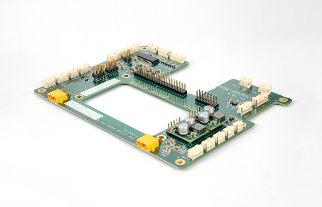
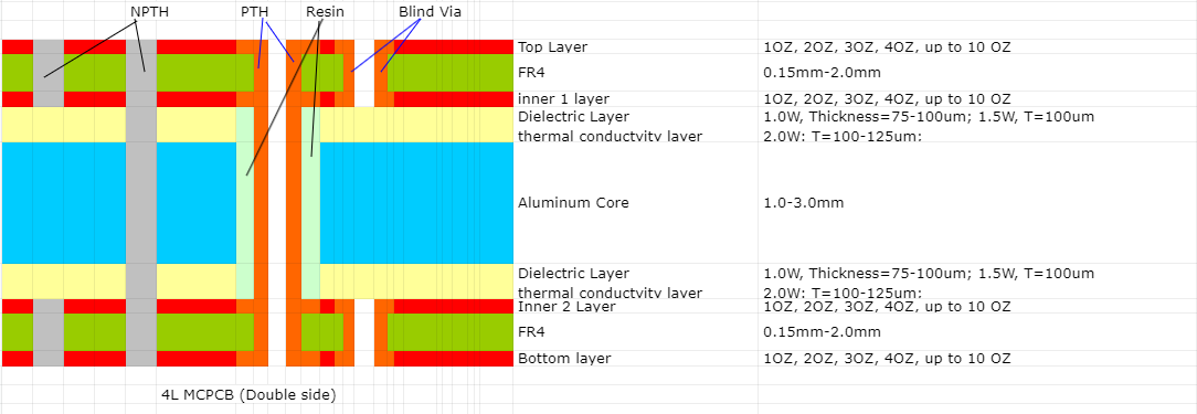
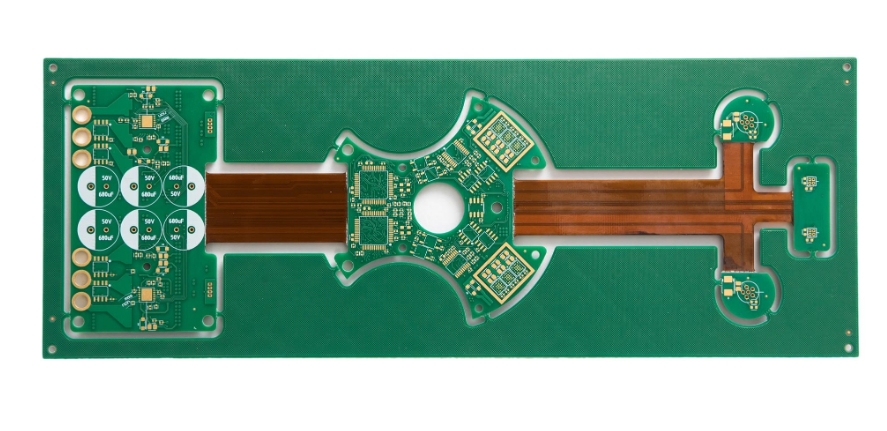
Rigid flex pcb,rigid-flex printed circuit board,Rigid flex circuit are a hybrid construction flex circuit consisting of rigid and flexible substrates which are laminated together into a single structure. Each layer of rigid-flex circuit are electrically interconnected by plated through holes (PTH), which is different from a flexible circuit with FR4/PI stiffener on top or bottom of flex circuit only by the means of presensive or thermal senstive adhesive only, no PTH.
Rigid-flex PCBs can be divided into single-sided boards, double-sided boards and multi-layer boards according to the number of conductive circuit layers. Multi-layer boards usually contain multiple rigid layers and flexible layers, and the circuits are connected and interconnected through interlayer connections.
Is Rigid flex PCB reliable?
- Design and manufacturing efficiency: Designers of rigid-flex boards can use a single component to replace a composite printed circuit board connected by multiple connectors, multiple cables and ribbon cables, which not only has stronger performance and higher stability, but also limits the scope of the design to one component, optimizing the available space by bending and folding the lines like a stacked paper swan.
- Space and weight optimization: In PCB prototyping for consumer electronics, the use of rigid-flex boards not only maximizes space use and minimizes weight, but also greatly improves reliability, eliminating many needs for solder joints and fragile and fragile wiring that are prone to connection problems. The design of this circuit board allows the size and weight of equipment and systems to be reduced while maintaining functionality.
- High stress environment adaptability: Rigid-flex boards also have high impact resistance and can survive in high stress environments, which makes it widely used in military, aviation and medical equipment.
- Excellent electrical performance: Rigid-flex boards provide excellent electrical performance, and good thermal conductivity makes components easy to cool. The lower dielectric constant of the flexible part allows for fast transmission of electrical signals, and the PI substrate has a higher glass transition temperature or melting point, which allows the components to operate well at higher temperatures.
- Assembly reliability: Rigid-flex boards reduce the hardware required for traditional rigid boards and flexible boards to be connected, such as traditional jumper sockets, etc., and can provide higher assembly reliability.
What is the difference between rigid flex and semi flex?
- Definition and structure
Rigid-flexible board: It is a combination of soft board and hard board, that is, a thin layer of flexible bottom layer and rigid bottom layer are combined and laminated into a single component to form a circuit board1. It changes the traditional flat design concept and expands it to a three-dimensional space concept. It has both rigid layer and flexible layer and is a multi-layer printed circuit board.
Semi-flexible board: It is a PCB used in the field of static bending obtained by combining controlled deep milling or rigid-flexible board processing technology (such as milling cover or opening window, etc.) in the standard hard board processing process2. It often uses FR4 material, first processes the PCB according to the normal process, and then mills the middle part that needs to be bent to make it flexible. - Flexibility and application
Rigid-flexible board: It has higher flexibility and can be bent, folded or rounded, and then integrated into various products, such as aerospace equipment, military aircraft, high-end medical equipment, digital cameras, portable cameras and high-quality MP3 players.
Semi-flexible board: Although it can be bent or curved, its flexibility is not as good as that of rigid-flexible board. It is mainly used in situations where static bending is required, such as endoscopes in medical equipment, injection needle tip protection circuit boards, and medical equipment temperature control circuit boards. - Processing and cost
Rigid-flexible board: Due to the mixed use of multiple materials and multiple production steps, its processing time is longer and the production cost is higher.
Semi-flexible board: Although its processing process is also more complicated, its processing cost is lower than that of rigid-flexible board, and it is more suitable in some applications. - Features and advantages
Rigid-flexible board: It has stronger performance and higher stability, can reduce space and weight, and improve the reliability of connection. - Semi-flexible board: It has the advantages of low cost, good dimensional stability, bendable three-dimensional installation to reduce space, and reduce the number of interfaces during assembly to improve reliability.
how do they add rigid layers to flex pcb?
- Design layout: Before starting the manufacturing process, the PCB design layout is first carried out to determine the location and connection method of the components.
- Substrate preparation: Clean the laminate containing the copper layer to prepare for the subsequent manufacturing process.
- Pattern generation: The generation of circuit patterns is completed by screen printing or photo imaging.
- Etching process: The laminate with the circuit pattern is soaked in an etching tank or sprayed with an etchant solution for etching.
- Mechanical drilling: Circuit holes, pads and via patterns are drilled using a precision drilling system or technology, such as laser drilling technology.
- Copper plating process: Deposit the required copper in the plated vias to establish electrical interconnections between layers.
- Covering layer application and lamination: Apply the covering layer material (such as polyimide film) and adhesive, and laminate under specific temperature, pressure and vacuum limits to ensure proper adhesion of the covering layer.
- Apply stiffeners: Apply local additional stiffeners before additional lamination processes as required by the board design.
- Flexible board cutting: Cut flexible boards from production panels using hydraulic punching methods or specialized punching knives.
- Electrical testing and verification: Conduct electrical testing in accordance with IPC-ET-652 guidelines to confirm that the insulation, connection, quality, and performance of the circuit board meet the requirements of the design specifications.
What are the disadvantages of rigid flex PCB?
- Material damage or breakage: The flexible materials used in rigid-flex boards are susceptible to flexure and bending. Long-term use or improper handling may cause damage or breakage of the flexible part, resulting in an open circuit.
- Poor welding: The manufacture of rigid-flex boards requires welding processes. If the welding is poor or the solder joints are of poor quality, it may cause loose connections or solder joints to fall off, resulting in an open circuit.
- Excessive bending or stretching: Excessive bending or stretching during use may cause the connection wires or wires of the flexible part to be stretched excessively and break, causing an open circuit.
- Design defects: If the design of the rigid-flex board is unreasonable or defective, such as insufficient design of the overbending area or too small bending radius, the material of the flexible part may be damaged by excessive stress, resulting in an open circuit.
- Environmental factors: Under different environmental conditions, it may be affected by factors such as temperature, humidity, and chemicals. Long-term use in harsh environments may cause material aging or corrosion, resulting in an open circuit.
- Damage during assembly: During the assembly process, improper operation or external force may cause damage to the connecting wires or wires of the flexible part, resulting in an open circuit.
Application fields of rigid flex PCB
- Automotive electronics: Rigid-flex boards are widely used in automotive electronic systems such as dashboards, navigation systems, and in-car entertainment systems in the automotive industry. Their flexibility and high reliability enable them to adapt to the complex spatial layout and vibration environment inside the car.
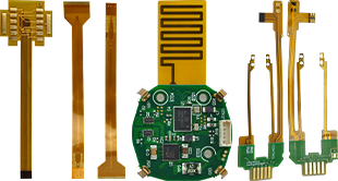
- Medical equipment: In the field of medical equipment, rigid-flex boards also have important applications, such as medical monitoring equipment, medical imaging equipment, etc. Its flexible part can adapt to different equipment shapes and size requirements, while having stable circuit connection performance.
- Aerospace field: Rigid-flex boards are usually used in aircraft dashboards, navigation systems, communication equipment, etc. in the aerospace field. Due to their light, thin and flexible characteristics, rigid-flex boards have become an ideal choice for aerospace equipment.
- Smart wearable devices: With the rapid development of smart wearable devices, rigid-flex boards are widely used in products such as smart watches and health monitoring equipment. They can be combined with curved display screens, sensors and other components to achieve a more humanized design.
- Industrial control field: In the field of industrial automation control, rigid-flex boards are often used in PLC controllers, robot control systems, sensor interfaces, etc. Its flexibility and reliability ensure the stable operation of the equipment in harsh environments.

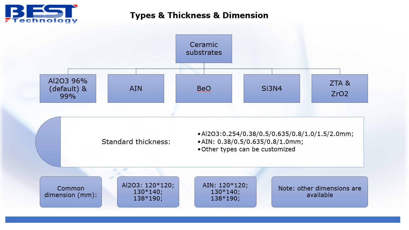
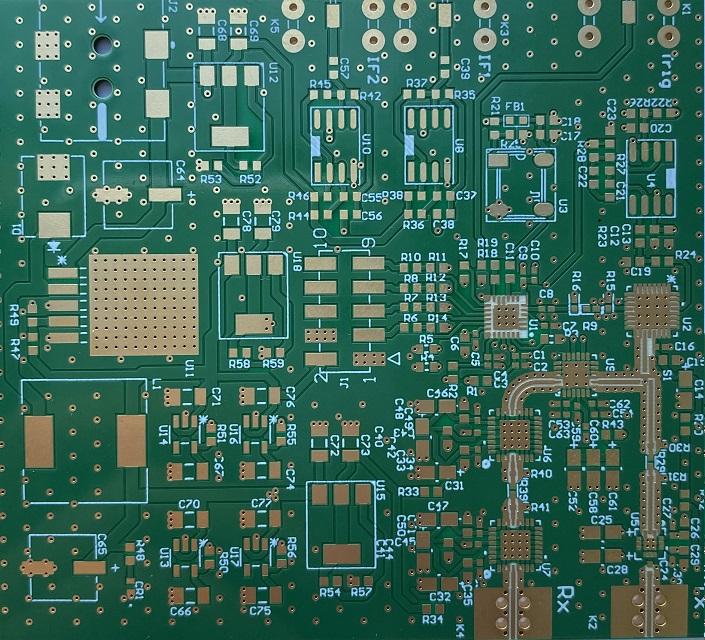
Rigid flex pcb manufacturer
rigid flex pcb.rigid-flex printed circuit board,Rigid flex circuit are a hybrid construction flex circuit consisting of rigid and flexible substrates which are laminated together into a single structure. Each layer of rigid-flex circuit are electrically interconnected by plated through holes (PTH), which is different from a flexible circuit with FR4/PI stiffener on top or bottom of flex circuit only by the means of presensive or thermal senstive adhesive only, no PTH.

Multilayer circuitry-from 3 to 14+ layers
Min LW/LS: 4mil/4mil
Adhesive-based and adhesiveless constructions, including thermoplastic and thermoset stiffener attachment.
Polyimide substrates: 1/2mil – 4mil
Copper: 1/3OZ – 2OZ, RA or ED type
Stiffeners include Polyimide (0.075-0.20mm), FR4 (0.15-2.0mm), and punched or formed metal parts (0.075-1.0mm)
Low-cost, conventional fabrication and lamination completed with PTH based plating
Screened inks, photo-imageable soldermasks, or laminated coverlay dielectrics
Surface finishes: ENIG, electroplated nickel/gold, immersion silver, tin,
EMI Shielding
how to design flex rigid pcb?
Rigid-Flex Circuit Design Guidelines
To form a rigid-flex, follow these considerations to ensure the best results.
Considerations When Designing Rigid-Flex Circuits
To produce a rigid-flex PCB with unmatched quality and functionality, you must follow the correct manufacturing specifications. This is the set guidelines and standards that manufacturers must consider when designing and manufacturing flexible circuit boards.
Determine Manufacturing Process and Materials Beforehand
Depending on the flexibility you require, you need to decide beforehand what materials to use and the methods to use. Example; When the board you are designing only needs to be folded during manufacturing and thereafter be in a fixed position without bending, you can decide the following
- Copper type and grade
- Manufacturing method
- Number of layers to be used.
On the other hand, if the board is for an application with frequent movement, vibration, and impact, you must be clear in choosing the following:
- Copper Coils
- Adhesives and
- Number of Layers
Place Copper Traces at Right Angles to Rigid-Flex
Copperworks is a great fit when placed on the right edge of the board. Avoid bending copper traces at corners as it will pull stress and may not create the best bend. For PCB flex that requires bending, use sharp radius bends to avoid smudging copper traces.
Provide adequate pad support for exposed copper
Repetitive stress from frequent bending can cause copper on the circuit to break away from the polyimide substrate. Support exposed copper with pads to prevent separation.
Use hatched polygons
Hatched polygons instead of solidified copper help maintain the flexibility of flexible PCBs.
Leave at least 1/2mm gap between copper ring and adjacent vias
1/2mm helps avoid fatigue caused by frequent bending. Placing vias in fixed areas of the board helps avoid frequent movement and bending, resulting in the best rigid-flex.