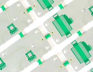
What is PCB Antenna?
PCB antennas are antennas printed directly onto a circuit board. Instead of using traditional wires, the copper traces on the PCB act as the antenna structure. This approach saves space and integrates the antenna directly into the board layout. Many devices, especially wireless modules, use this method to reduce size, weight, and production costs.
Since the antenna is part of the PCB itself, designers can customize its shape to fit different products. Small IoT devices, smart home gadgets, and compact industrial sensors benefit greatly from PCB antenna. Their simplicity, cost-effectiveness, and easy integration make them widely used across industries.
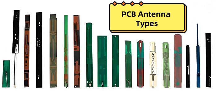
PCB Antenna Types
There are several PCB antenna types, each with different shapes and performance characteristics. The most common ones include:
1. Monopole PCB Antenna:
This type uses a single conductive element. It typically connects directly to a ground plane, often on the board itself. It offers good omnidirectional coverage, especially in compact designs.
2. Dipole PCB Antenna:
This antenna uses two conductive arms to form a balanced structure. It offers more predictable radiation patterns, making it ideal for communication devices that need reliable performance.
3. PIFA (Planar Inverted F Antenna):
This compact design works well when space is tight. It balances performance and size, often seen in mobile devices and compact IoT products.
4. Meander Line Antenna:
This type folds the antenna path into a compact shape. It reduces space but maintains effective length for desired frequencies.
5. Patch Antenna:
A simple flat copper section on the PCB, often used in high-frequency applications. It performs well for directional signals, especially in GPS and satellite devices.
How Does a PCB Antenna Work?
PCB antennas work by converting electrical signals into radio waves and vice versa. When a signal travels from the transmitter through the feed line into the antenna, the antenna radiates electromagnetic energy into the surrounding space.
On the receiving side, incoming radio waves induce small voltages in the antenna traces. The antenna feeds these signals into the receiver for processing.
The antenna’s size, shape, and layout determine the wavelengths it handles best. Smaller antennas typically suit higher frequencies. Antenna placement on the PCB also matters. Edge placement often helps, reducing interference from nearby components.
Designers carefully match the antenna impedance to the transmission line impedance. This matching reduces signal reflections and boosts energy transfer between the antenna and the wireless circuit.
How to Calculate Antenna Parameters?
When designing PCB antennas, getting accurate parameters matters a lot. These values help the antenna perform well across the required frequencies. Each type of antenna has unique needs, but some formulas apply to most designs. Here are the formulas to calculate each parameter.
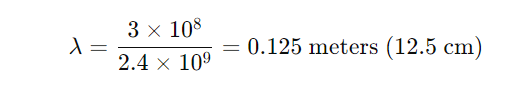
1. Wavelength (λ) Calculation
Wavelength helps you know how long your antenna should be. The formula is:

- λ is the wavelength (meters)
- c is the speed of light (about 3×10^8 meters per second)
- f is the frequency (Hertz)
For example, if you design for 2.4 GHz WiFi, the wavelength would be:
2. Impedance Matching
Impedance matching avoids signal loss at the connection point. This helps you decide how wide the antenna trace should be to keep signals clean. The ideal target for many PCB antennas is 50 ohms. The formula for a microstrip line impedance is:
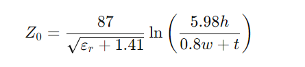
- Z₀ is the characteristic impedance (ohms)
- εr is the dielectric constant of your PCB material
- h is the height of the substrate (meters)
- w is the trace width (meters)
- t is the trace thickness (meters)
3. Antenna Gain Calculation
Antenna gain tells you how well the antenna focuses power in a preferred direction. If your design focuses well in one direction and uses materials with low loss, gain increases. It’s linked to directivity and efficiency using this formula:

- G is the gain (unitless or dBi if converted)
- D is the directivity (unitless)
- η is the efficiency (percentage as decimal)
4. Effective Aperture
Effective aperture shows how much power the antenna captures from a passing wave. The formula is:

- Aₑ is the effective aperture (square meters)
- λ is the wavelength (meters)
- G is the antenna gain (unitless)
5. Bandwidth
Bandwidth measures the range of frequencies the antenna supports, it helps devices work under changing conditions. For many PCB antennas, the fractional bandwidth works better:

- BW is the fractional bandwidth (percent)
- fₕᵢgₕ is the upper frequency limit (Hertz)
- fₗₒw is the lower frequency limit (Hertz)
- fₐₗₐₜₑr is the center frequency (Hertz)
6. Radiation Efficiency
This tells you how much power leaves the antenna versus what gets lost. High-efficiency designs waste less power inside the PCB. It’s calculated using:

- η is the efficiency (decimal or percentage)
- Pₐₐₐ is radiated power (watts)
- Pₐₙₚₐₜ is input power (watts)
7. Return Loss
Return loss shows how much power reflects back into the feed line instead of radiating out. The formula is:

- RL is return loss (dB)
- Γ is the reflection coefficient (unitless)
The reflection coefficient itself comes from:

- Zₐₐ is the antenna input impedance (ohms)
- Z₀ is the system impedance (ohms, often 50 ohms)
- A return loss better than -10 dB is usually considered acceptable.
What is the Frequency of a PCB Antenna?
The operating frequency of a PCB antenna depends mainly on its length, shape, and the dielectric constant of the substrate. Many PCB antennas operate in common wireless bands like:
- 2.4 GHz: Used for Wi-Fi, Bluetooth, and many IoT devices.
- 5 GHz: Also used for Wi-Fi, offering faster speeds in exchange for shorter range.
- 868 MHz and 915 MHz: Popular for LoRa and other low-power, long-range applications.
- 1.575 GHz: Used in GPS systems.
PCB antennas designed for these bands follow specific length and width guidelines to match the target frequency. Designers also account for the substrate material and thickness, which shift the actual frequency slightly compared to calculations.
What is the Gain of a PCB Antenna?
Antenna gain measures how much power concentrates in a specific direction compared to a perfect reference antenna. PCB antenna gain varies widely depending on design type and size.
Monopole PCB antennas often have gain around 0-2 dBi, providing wide coverage.
Patch antennas, with directional focus, may offer gains from 3 to 7 dBi.
PIFA antennas, designed for compact spaces, often land in the 0 to 3 dBi range.
Higher gain antennas focus more energy, improving range in certain directions. Lower gain designs spread energy more evenly, supporting omnidirectional coverage in devices like routers and sensors.
Difference Between Wire Antenna and PCB Antenna?
Wire antennas use external conductive elements, often flexible or rigid metal wires. These antennas perform well across a wide range of frequencies and offer good efficiency when properly tuned. They are easier to reposition and optimize after manufacturing.
PCB antennas integrate directly into the board. They offer compact, low-cost solutions for devices where space matters. Their performance ties closely to PCB material, layout, and nearby components. Adjustments after production are difficult.
Wire antennas suit devices needing adjustable range or performance. PCB antennas fit compact, high-volume designs where cost, size, and integration matter more.
PCB WiFi Antenna Design Guide
Designing a WiFi antenna on a PCB needs both planning and understanding of basic RF principles. It’s not just about drawing a shape on the board. Every part of the design affects how well the antenna works — from the trace width to the ground plane.
1. Select the frequency band – 2.4 GHz, 5 GHz, or both.
2. Choose antenna type – monopole, meander, or patch.
3. Define layout space – allow enough clearance for antenna traces and ground plane.
4. Match impedance – aim for 50 ohms.
5. Simulate performance – check radiation pattern, gain, and efficiency.
6. Prototype and test – measure real-world performance.
Careful placement near board edges and avoiding large nearby metal parts helps maximize performance. Ground plane design also affects gain and efficiency.
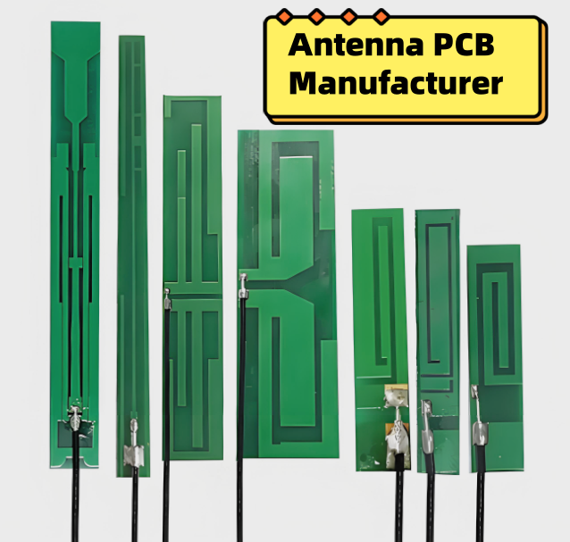
Your Reliable OEM PCB WiFi Antenna Manufacturer – Best Technology
When choosing an Antenna PCB Manufacturer, you need experience, precision, and flexibility. At Best Technology, we have over 18 years of PCB manufacturing experience, serving industries from telecom to industrial IoT.
Our team supports custom PCB WiFi antenna designs, ensuring performance matches your product’s needs. Whether you need compact PIFA antennas or high-gain patch designs, we provide end-to-end support, from design advice to mass production.
As one of the trusted OEM PCB WiFi antenna manufacturers in China, we focus on quality, fast delivery, and customer satisfaction. Contact us to discuss your project and see why companies worldwide trust Best Technology for reliable PCB WiFi antenna manufacturing. For more information about PCB technology, welcome to contact us at sales@bestpcbs.com.