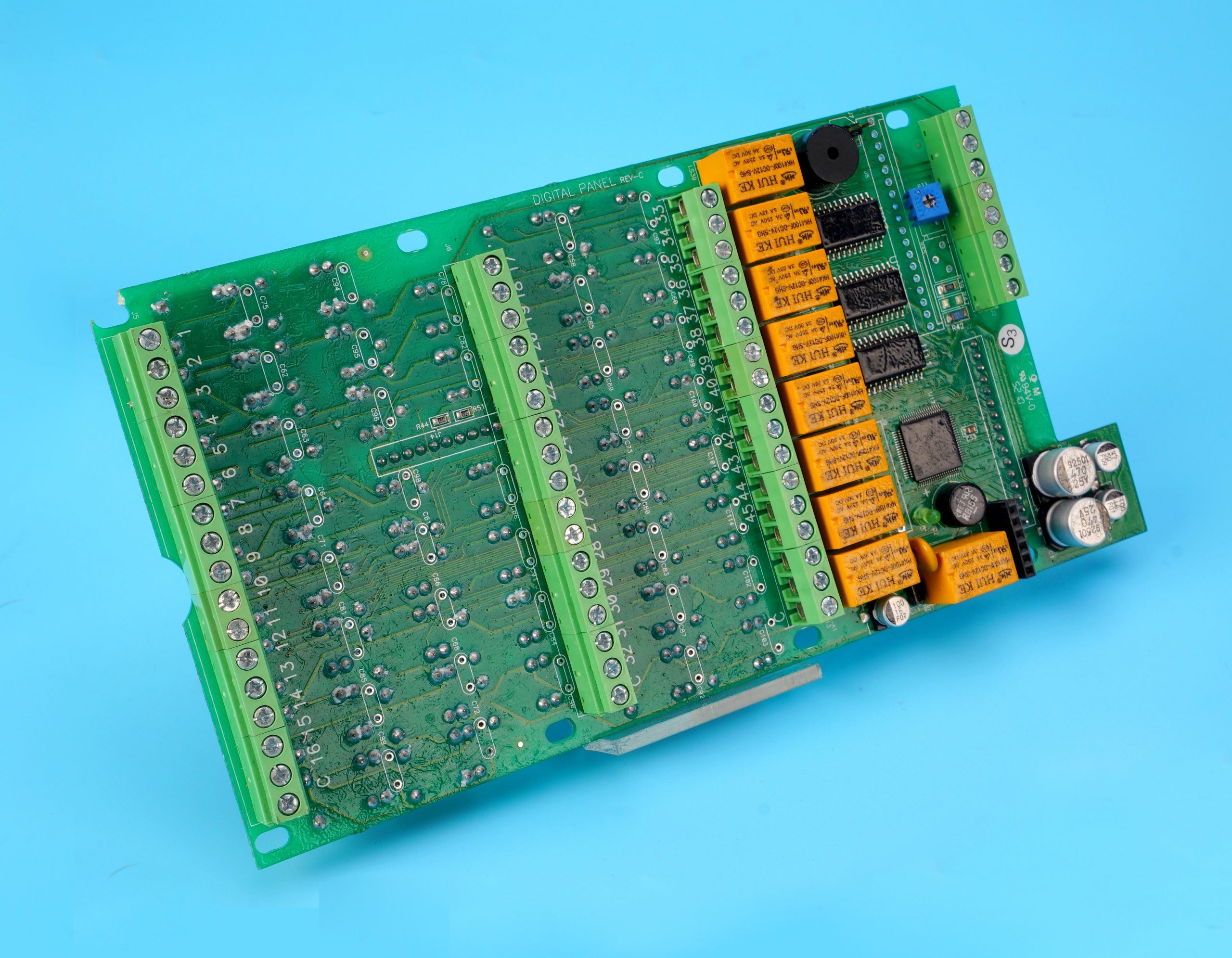
PCB assembly requirements include ensuring that the size and positioning of the PCB board meet the design specifications, reasonably arranging components, strictly controlling the soldering temperature, and performing quality inspections and tests through automatic inspection equipment to ensure that the circuit connections are correct and the components are firmly soldered, thereby ensuring the quality and reliability of the product.
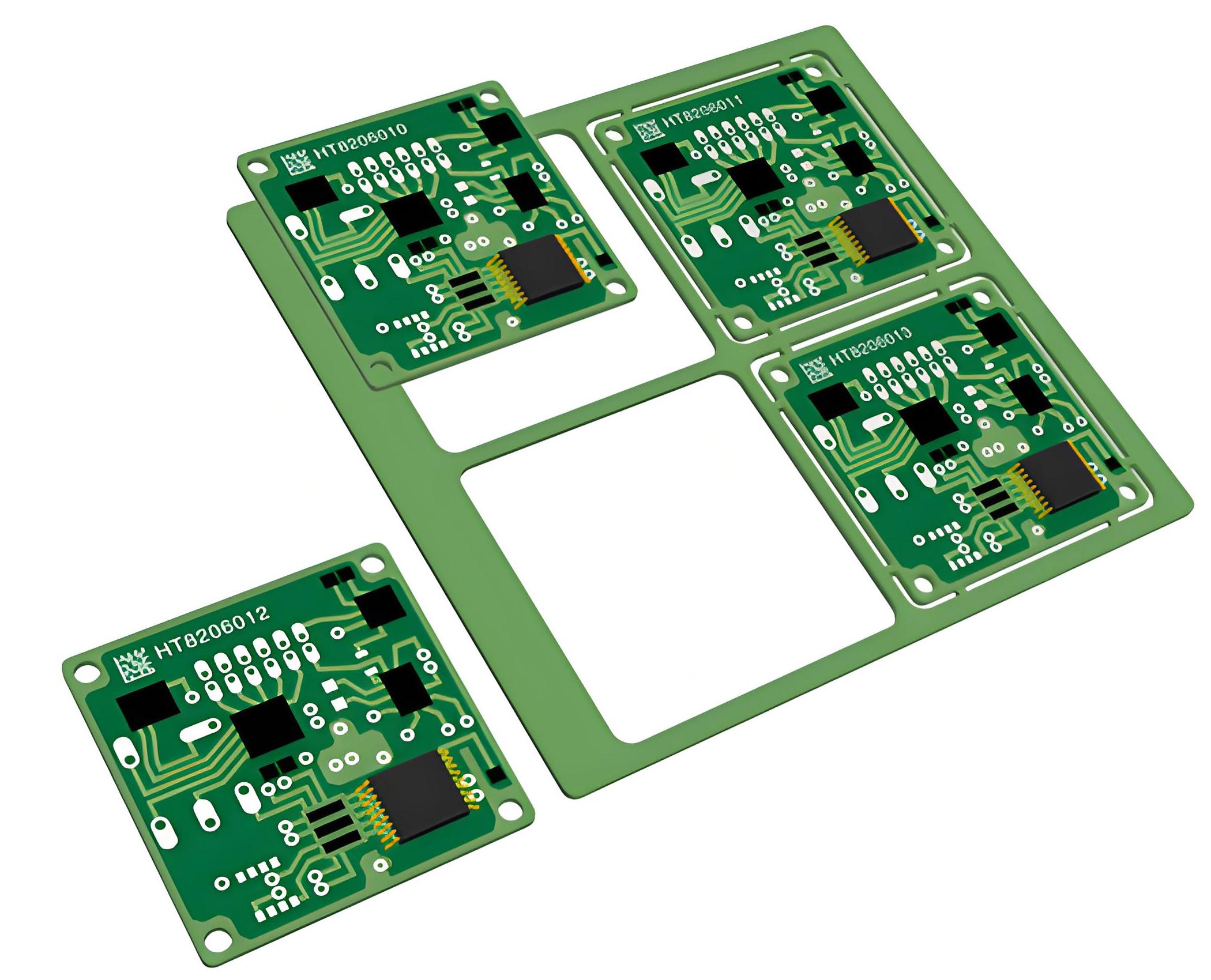
What is PCB panelization?
PCB panelization refers to the process of grouping multiple PCB designs into a larger “panel” or array. This is done to optimize manufacturing efficiency and minimize the cost of the assembly process.
Panelization is particularly useful when dealing with small-sized PCB designs. By panelizing the design, manufacturers can perform soldering, testing, and other assembly processes on a group of PCBs simultaneously, which reduces the overall cost of assembly.
What are the types of panels for PCB assembly?
There are several types of panels used for PCB assembly. The main types include:
- V-Scored Panels: These panels are made by scoring the PCB at specific points, creating a groove that makes it easy to separate the individual PCBs after the assembly is complete.
- Tab-Routed Panels: Tab-routing is a process where the PCB is connected to the panel with small tabs. After assembly, these tabs are cut to separate the individual PCBs.
- Laser-Routed Panels: In laser routing, a laser is used to precisely cut around the edges of the PCB. It offers high precision and is typically used for high-density designs or sensitive applications where a more precise separation method is needed.
- Combo Panels: These panels combine the benefits of V-scoring and tab-routing, allowing for a flexible approach to assembly and separation.
What are the panel requirements for PCB assembly?
Panel requirements are a set of guidelines and specifications that need to be followed during the PCB panelization process to ensure that the final assembly is accurate, efficient, and cost-effective. These requirements include:
- Panel Size: The size of the panel should be optimized to fit into the equipment used during assembly (like pick-and-place machines).
- Edge Clearance: The edge of the PCB should have enough clearance to prevent mechanical stress and interference during the manufacturing process.
- Component Placement: Panels should be designed so that the components are placed efficiently. This includes keeping components within the panel’s accessible area for automated assembly machines.
- Separation Strategy: Whether using V-scoring, tab-routing, or laser routing, the method chosen for separating the individual boards after assembly must be considered in the panelization process.
- Manufacturing Tolerances: All panels should adhere to strict tolerances to ensure the accuracy and quality of the final product. This includes positioning of components, trace width, and hole sizes.
What is the standard for PCB assembly?
The standard for PCB assembly is typically guided by established organizations such as IPC (Institute for Printed Circuits), which provides standardized rules for PCB design, assembly, and testing. For example:
- IPC-2221 provides guidelines for designing printed boards and other forms of component mounting.
- IPC-A-610 outlines the acceptability requirements for electronic assemblies, including things like solder joints, component placement, and cleanliness.
- IPC-2222 addresses the design requirements for multi-layer PCBs.
These standards ensure that PCBs meet performance, quality, and safety requirements. Adhering to these guidelines helps manufacturers produce high-quality products that are reliable and meet industry expectations.
What files are required for PCB assembly?
To ensure a smooth PCB assembly process, manufacturers typically require several key files. These files provide the necessary data to fabricate, assemble, and test the PCB. Some of the most important files include:
- Gerber Files: These files contain the information necessary to produce the copper layers of the PCB, including the layout of the traces, pads, and vias.
- Bill of Materials (BOM): The BOM is a detailed list of all components required for the PCB, including part numbers, values, and descriptions.
- Pick and Place Files: These files contain the positions of the components on the PCB, allowing automated machines to place the components accurately.
- Schematic Files: Schematic files show the circuit design and connectivity between components. These are essential for verifying that the assembly process follows the correct electrical design.
- Stencil Files: If solder paste is required, stencil files guide the application of the paste to the PCB.
Having all of these files ensures that the assembly process runs smoothly and that the final product is built to the correct specifications.
What is the PCB assembly process?
The PCB assembly process involves several steps, each of which must be carried out with precision to ensure the board works properly. The general process is as follows:
- Solder Paste Application: The first step involves applying solder paste to the PCB pads using a stencil.
- Component Placement: Automated pick-and-place machines place the components onto the PCB.
- Soldering: Once the components are placed, the PCB moves into a reflow oven or wave soldering machine, where the solder paste is heated, melting the solder and attaching the components to the board.
- Inspection: After soldering, the PCB is inspected to ensure that the components are securely attached, and there are no issues like solder bridges or cold joints. Visual inspection, X-ray inspection, or automated optical inspection (AOI) may be used.
- Testing: The PCB undergoes electrical testing to verify its functionality. This may include functional tests or in-circuit tests.
- Final Touches: After passing tests, the PCB is cleaned, and any excess solder is removed. It may also undergo further inspection to check for cosmetic defects.
- Packaging and Shipping: Finally, the completed PCBs are packaged and shipped to the client.
What are the tolerances for PCB assembly?
Tolerances are the allowable variations in the dimensions and placement of components during the assembly process. These tolerances must be carefully controlled to ensure that the PCB works as intended.
Common tolerances include:
- Component Placement: The precision with which components are placed on the PCB is crucial. Typically, the tolerance for placement accuracy is around ±0.1mm, but it can vary based on the size and type of components.
- Trace Width: PCB traces need to be within certain width tolerances to handle the required current and ensure proper signal integrity.
- Hole Sizes: The diameter of holes for through-hole components must be accurate to ensure proper insertion and soldering.
What is the component clearance for PCB assembly?
Component clearance refers to the amount of space between the components on the PCB. It’s essential for ensuring that components don’t interfere with each other during the assembly process.
Sufficient clearance is also important to avoid issues like short circuits or mechanical stress that could damage components.
Clearance requirements vary depending on the component size and type. For example, smaller components may require tighter spacing, while larger components need more room to ensure proper soldering and prevent overheating.
Conclusion:
PCB assembly is a complex process that involves careful planning, precise design, and stringent manufacturing standards. Panelization, assembly requirements, tolerances, and component clearance all play vital roles in ensuring a successful assembly process.
If you’re looking for professional PCB assembly services that meet industry standards and provide top-tier results, Best Technology is here to assist you. Get in touch with us at sales@bestpcbs.com to discuss your PCB assembly needs.