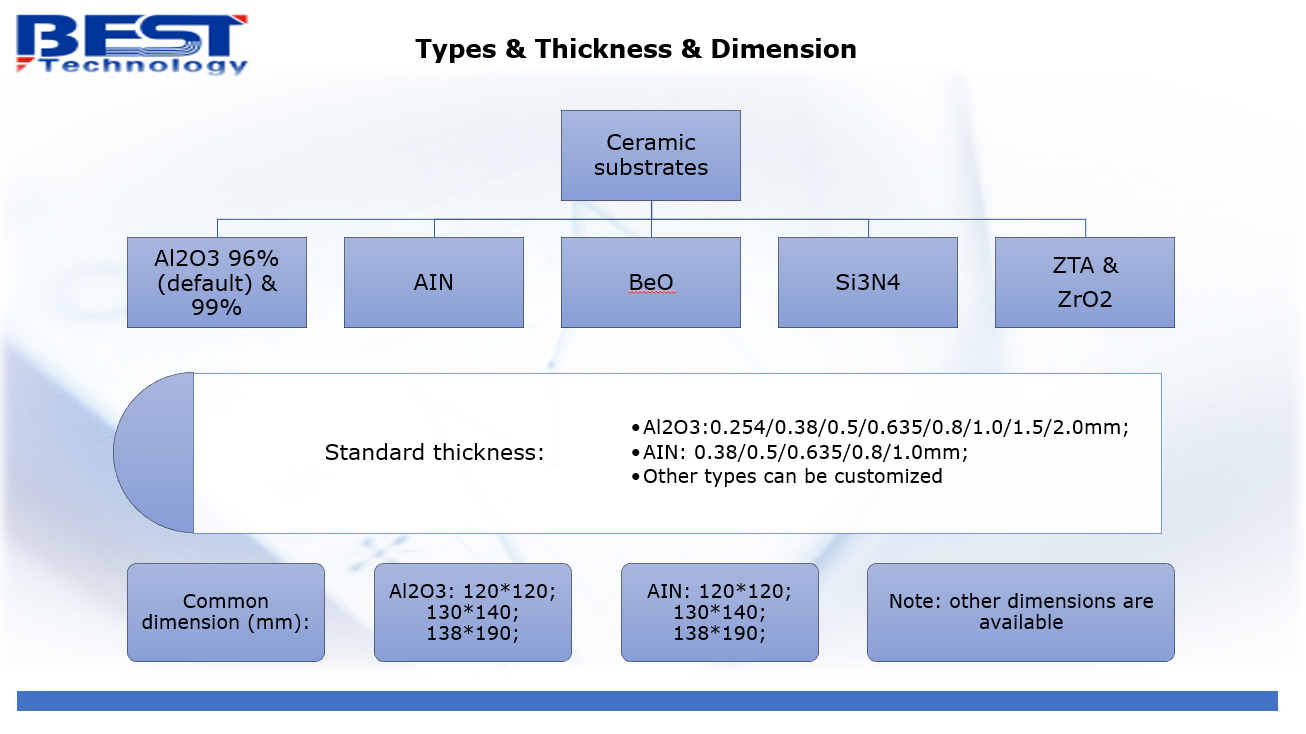
The top ten commonly used ceramic materials:
Common ceramic circuit board materials mainly include 96 aluminum oxide (Al2O3), 99 aluminum oxide (Al2O3), zirconium oxide (ZrO2), aluminum nitride (AlN), silicon carbide (SiC), silicon nitride (Si3N4), piezoelectric ceramics, diamond, sapphire, toughened ceramics (ZTA).
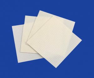
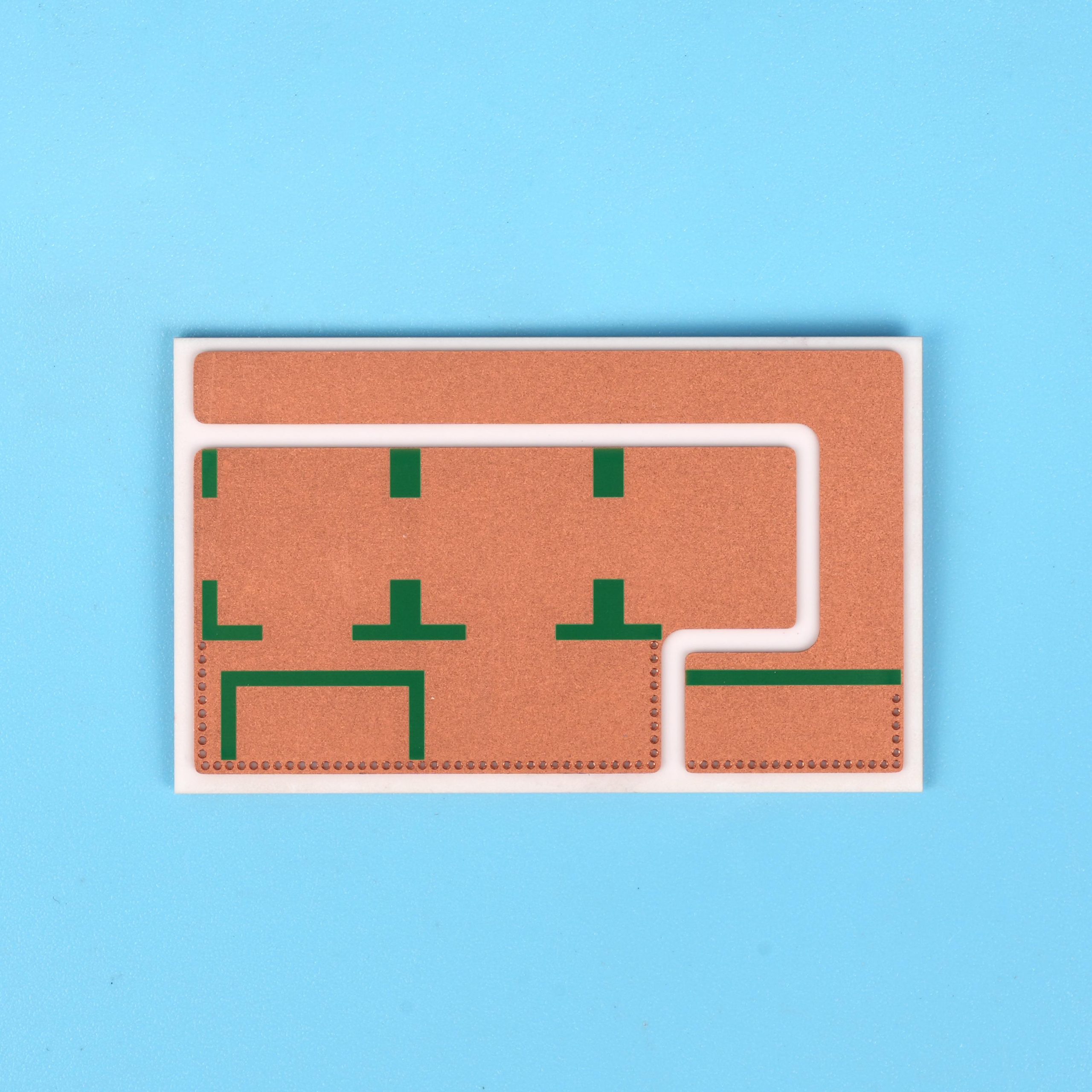
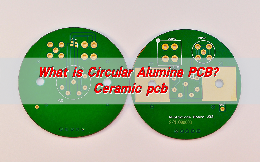
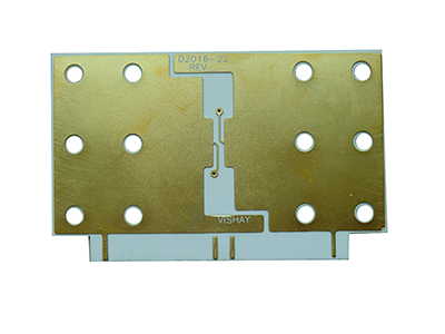
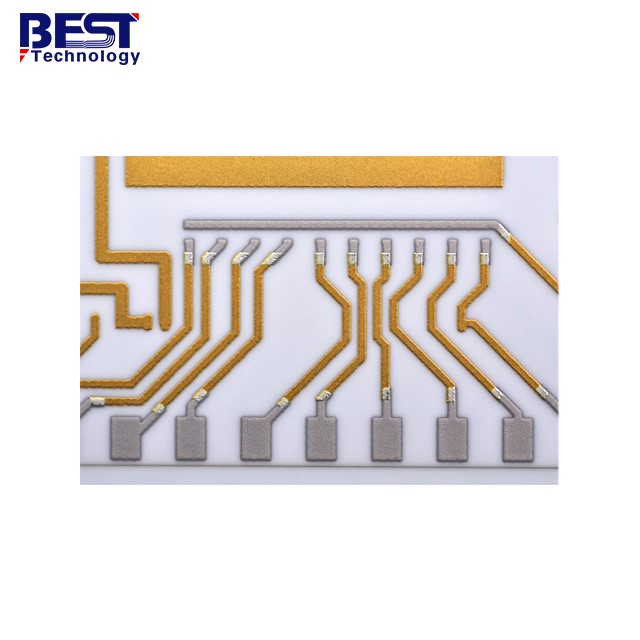
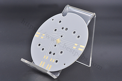
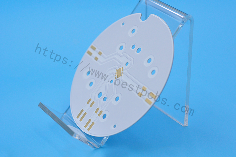
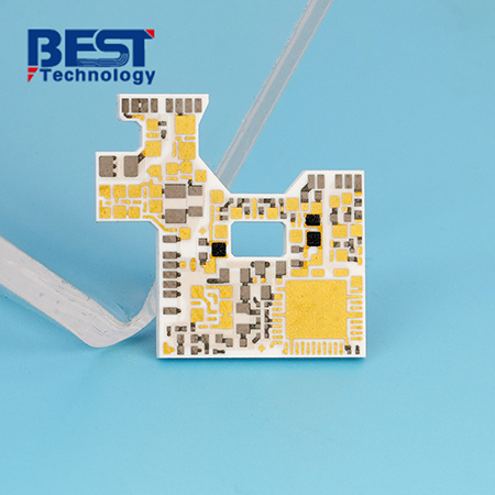
Ceramic PCB Material
Uncommon ceramic circuit board materials
Uncommon ceramic circuit board materials mainly include silicon dioxide (SiO2), titanium zirconium oxide (ZrTiO4), boron nitride (BN), boron carbide (B4C), magnesium oxide (MgO), iron oxide (Fe2O3), cerium oxide (CeO2), silicon nitride (Si3N4), yttrium zirconium oxide (Y2O3-ZrO2), yttrium aluminum oxide (Y3Al5O12), titanium oxide (TiO2), silicon zirconium oxide (ZrSiO4), tungsten carbide (WC), titanium carbide (TiC), titanium nitride (TiN), silicon nitride (SiOxNy).
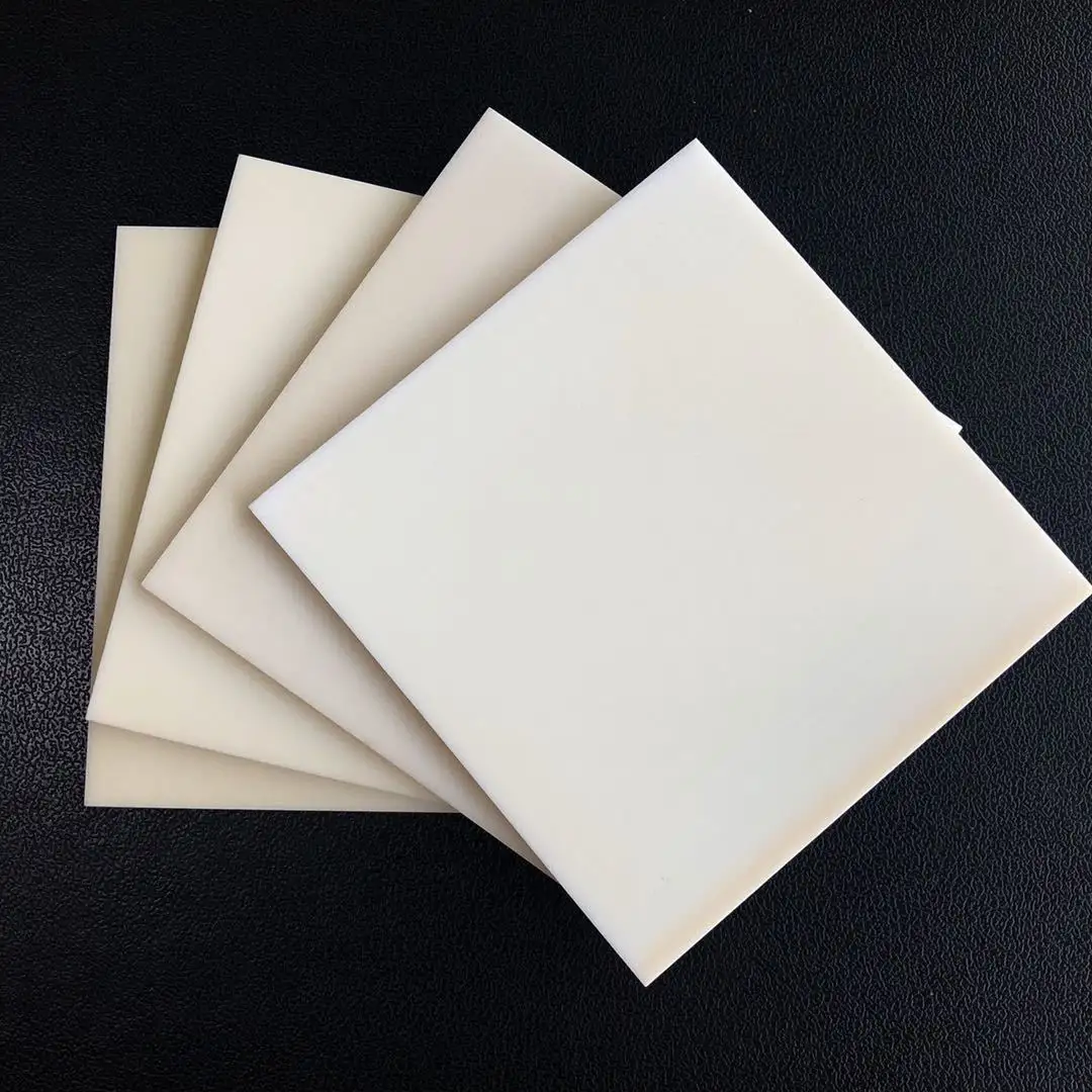
Alumina ceramic materials
Alumina ceramic materials
1). 99 alumina
99 alumina refers to alumina materials with a purity of 99% or higher. It is usually made of chemically pure alumina or high-purity alumina as raw materials, and is made through multiple processes such as high-temperature calcination, crushing, molding, and sintering. Compared with 96 alumina, 99 alumina has higher chemical purity, density and hardness, as well as better high-temperature stability and corrosion resistance.
99 alumina is widely used in electronics, machinery, chemical industry, aerospace and other fields. In the electronics field, 99 alumina is usually used to manufacture high-frequency electronic components, integrated circuit packaging, dielectrics and other devices; in the mechanical field, 99 alumina is mainly used to manufacture high-hardness ceramic tools, bearing balls, etc.; in the chemical field, 99 alumina can be used to manufacture catalysts and adsorbents; in the aerospace field, 99 alumina is often used to manufacture high-temperature structural parts, aircraft engine parts, etc.
2). 96 alumina
96 alumina, also known as industrial alumina or α-alumina, is a high-purity ceramic material. Its chemical formula is Al2O3, which belongs to oxide ceramics. 96 alumina is usually made of alumina powder through pressing, molding, sintering and other processes. The “96” here means that its aluminum oxide purity reaches more than 96%. 96 alumina has the characteristics of high hardness, high strength, high wear resistance, and good high temperature stability. It is widely used in the manufacture of ceramic products, refractory materials, abrasives, electronic devices and other fields.
Advantages of 99 alumina substrate:
High purity, usually reaching a purity level of 99.99%, excellent electrical properties, high dielectric constant and low dielectric loss.
Good high temperature stability, can work stably in high temperature environment, and can usually withstand temperatures up to 1700℃.
High mechanical strength, high strength, high hardness, not easy to be damaged, and can withstand greater force and pressure.
It has excellent corrosion resistance, is not corroded by most chemical substances, and is suitable for chemical media such as acids and alkalis.
It can be prepared into a thinner substrate, which is conducive to the preparation of microelectronic devices.
Advantages of 96 alumina substrate:
Cheaper than 99 alumina substrate, the cost is relatively low.
It is easier to process than 99 alumina substrate, and can be processed by cutting, drilling and other processing, which is convenient for preparing substrates of various shapes.
In some low-temperature and low-electric field strength applications, the dielectric constant and dielectric loss are lower than those of 99 alumina substrate, and it has better signal transmission performance.
Disadvantages:
Compared with 99 alumina substrate, 96 alumina substrate has lower purity, higher dielectric constant and dielectric loss.
It is prone to brittle fracture in high temperature environment.
Alumina ceramic application industry
99 alumina substrate: suitable for high-power LED, high-voltage integrated circuit, high-temperature sensor, high-frequency electronic components and other fields.
96 alumina substrate: suitable for low-power electronic components, sensors, capacitors, micro relays, microwave components and other fields.
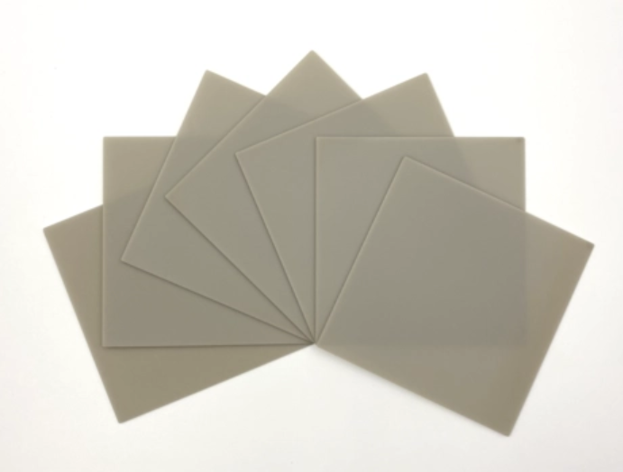
Aluminum nitride ceramic material (AlN)
Aluminum nitride ceramic material (AlN)
Aluminum nitride ceramic is a high-performance ceramic material made of aluminum nitride powder sintered at high temperature. Its main component is aluminum nitride (AlN), which has the characteristics of high melting point (about 2800℃), hardness (9.0 to 9.5Mohs), strength and thermal conductivity. At the same time, it also has good insulation performance, chemical stability and high temperature resistance. Due to these characteristics, Sliton aluminum nitride ceramic circuit boards are widely used in microelectronics, optoelectronics, power electronics, aerospace and other fields.
Advantages
- High hardness: The hardness of aluminum nitride is close to that of diamond, which is more than 3 times that of traditional alumina. It can be used to make high-strength mechanical parts.
- High strength: Aluminum nitride has high strength, good wear resistance and corrosion resistance, and can be used to make high-load, high-wear and corrosion-resistant parts.
- High thermal conductivity: The thermal conductivity of aluminum nitride is very high, reaching 170-230W/(m·K), which is more than 4 times that of traditional aluminum oxide. It can be used to make high-power, high-frequency RF components.
- High insulation: The dielectric constant of aluminum nitride is low, about 1/3 of that of traditional aluminum oxide, and can be used to make high-frequency, high-precision microwave components.
- Anti-oxidation: Aluminum nitride has good anti-oxidation properties at high temperatures and can be used to make parts in high-temperature environments.
Application of aluminum nitride ceramics
Widely used in semiconductors, aerospace, electronics, military and other fields. For example, it is used to make high-frequency RF devices, microwave components, electronic ceramics, thermistors, high-temperature sensors, etc.
Zirconia ceramic material (ZrO2)
Zirconium oxide ceramic material is a ceramic material with high strength, high hardness, high temperature tolerance, corrosion resistance and good insulation performance. Its chemical formula is ZrO2, and it is usually stabilized to improve the stability and wear resistance of its lattice. Zirconia ceramic material has the characteristics of low thermal conductivity and high melting point, so it is widely used in industrial fields with strict requirements such as high temperature, high pressure, high speed and high precision, such as aerospace, electronics, medical and energy.
Advantages
- High hardness: The hardness of zirconia ceramics is very high, usually reaching HRA90 or above, even up to HRA95, which is more than 10 times that of steel.
- High strength: Zirconia ceramics have extremely high strength, which can reach 900MPa at room temperature, and can still maintain high strength at high temperature.
- Good wear resistance: Zirconia ceramics have high surface flatness and high hardness, so they have good wear resistance.
- Good corrosion resistance: Zirconia ceramics are chemically inert and not easily corroded by chemicals such as acids and alkalis, and can operate stably for a long time in harsh environments.
- Excellent insulation performance: Zirconia ceramics have excellent insulation performance and can be used for high-voltage insulation materials.
- Good high-temperature stability: Zirconia ceramics have extremely high melting points and high-temperature stability, and can be used for a long time in high-temperature environments.
Application of Zirconia Ceramics
Widely used in high-end manufacturing, electronics, aerospace, medical equipment, chemical industry and other fields, such as abrasives, high-temperature structures, pneumatic components, medical equipment, sensors, capacitors, etc.
Silicon carbide ceramic material (SiC)
Silicon carbide is a compound with the chemical formula SiC, which is composed of two elements: silicon and carbon. It is a ceramic material that is resistant to high temperature, corrosion, and extremely hard. It is also an industrial material widely used in extreme environments such as high temperature, high frequency, and high pressure. Silicon carbide has excellent mechanical, electromagnetic, and thermal properties, and is therefore widely used in semiconductors, disks, aerospace, and other fields. In addition, silicon carbide has good semiconductor properties and is also widely used in power electronics, optoelectronics, and other fields.
Advantages
- High hardness: The hardness of silicon carbide material is 5 times higher than that of steel and 3 times higher than that of aluminum.
- High strength: The strength of silicon carbide material is high, and the tensile strength can reach more than 400MPa.
- High temperature resistance: Silicon carbide material has a high melting point and can withstand high temperature thermal shock. The general use temperature is 1200℃-1600℃.
- Good oxidation resistance: Silicon carbide material can resist high temperature oxidation corrosion and can be used in air.
- Good wear resistance: Silicon carbide material has high hardness, low friction coefficient and good wear resistance.
- Good thermal conductivity: Silicon carbide material has excellent thermal conductivity, which is 2-3 times that of metal and can effectively dissipate heat.
- Good chemical stability: Silicon carbide material has good chemical stability and will not be corroded by acid, alkali, etc.
Silicon carbide ceramic PCB application
Widely used in high temperature, high pressure, high speed, high load, corrosion resistance and other fields, such as power, electronics, machinery, aviation, metallurgy and other industries.
Silicon nitride ceramic material (Si3N4)
Silicon nitride ceramic material is a high-temperature ceramic material based on nitrogen and silicon elements. It has excellent properties such as high strength, high hardness, high wear resistance, high temperature resistance, oxidation resistance, and corrosion resistance. Its chemical stability is extremely high and is not easily corroded by acids, alkalis, solvents, etc. The hardness of silicon nitride ceramic materials is comparable to that of diamond, or even higher, reaching about 24GPa. It is harder and less prone to wear than ordinary ceramic materials. At the same time, it has good insulation properties and thermal stability, and can work stably for a long time in high temperature environments.
Advantages of silicon nitride ceramic PCB materials
- High hardness: The hardness of silicon nitride ceramic materials is close to that of diamond, which can reach more than 30GPa.
- High strength: The bending strength of silicon nitride ceramic materials is high, which can reach more than 1000MPa.
- High wear resistance: Silicon nitride ceramic materials have good wear resistance and can be used to manufacture high-speed bearings and cutting tools, etc.
- High temperature resistance: Silicon nitride ceramic materials have high high temperature resistance and can be used in high temperature environments above 1000°C.
- Corrosion resistance: Silicon nitride ceramic materials have excellent corrosion resistance and can be used in some acidic and alkaline working environments.
- Lightweight: Silicon nitride ceramic materials are lighter than steel and can be used in lightweight design.
Silicon nitride ceramic PCB applications
Widely used in aerospace, optoelectronics, electronics, semiconductors, machinery and other fields.
Piezoelectric ceramic materials
Piezoelectric ceramic materials are ceramic materials with piezoelectric effect, which can deform under external electric field or mechanical stress, and generate electric charge when deformed. They are usually made of materials such as barium lead oxide (Pb(Zr,Ti)O3) or niobium lead oxide (Pb(Mg1/3Nb2/3)O3-PbTiO3) as the main components and sintered.
Advantages
- Piezoelectric effect: It can convert mechanical stress into electrical signals, or convert electrical signals into mechanical motion. This effect makes piezoelectric ceramic materials widely used in sensors, actuators, acoustic wave devices and other fields.
- Dielectric properties: With high dielectric constant and low dielectric loss, piezoelectric ceramic materials are used as capacitors, filters, etc. in electronic components.
- Mechanical properties: With high hardness, strength and wear resistance, piezoelectric ceramic materials are used in mechanical engineering.
- Thermal stability: With good thermal stability and high temperature resistance, it can work stably in high temperature environment.
Piezoelectric ceramic PCB applications
Widely used in sensors, actuators, acoustic wave devices, electronic components, mechanical engineering and other fields.
Diamond ceramic material
Diamond ceramic material is a new type of material made by sintering diamond powder and ceramic as raw materials at high temperature and high pressure. Because diamond has extremely high hardness, reaching Mohs hardness level 10, and has excellent wear resistance, corrosion resistance and high temperature oxidation resistance, diamond ceramic material has extremely high physical and chemical properties.
Advantages of diamond ceramic PCB material
- Extremely high hardness and strength, more wear-resistant, scratch-resistant and impact-resistant than ordinary ceramic materials;
- Excellent corrosion resistance, able to resist corrosive media such as strong acids and alkalis;
- Excellent high-temperature oxidation resistance, can be used for a long time at high temperature without damage;
- Excellent thermal conductivity and insulation performance;
- Easy to process into ceramic products of various shapes and sizes.
Application of diamond ceramic PCB
Diamond ceramic materials are widely used in high-end machinery, electronics, optics, medical and chemical fields, such as bearings, nozzles, cutting tools, hydraulic cylinders, electrical insulation parts, laser parts, etc.
Sapphire ceramic material
Sapphire ceramic material, also known as synthetic sapphire (Synthetic Sapphire), is a man-made single crystal material with excellent properties such as high hardness, high wear resistance and high corrosion resistance. The main component of sapphire ceramic material is aluminum oxide (Al2O3), which is prepared by melting or heat treatment at high temperature.
Advantages of sapphire ceramic material:
- High hardness: The hardness of sapphire ceramic material is second only to diamond, and it has high wear resistance.
- High corrosion resistance: Sapphire ceramic material has excellent corrosion resistance and can be used stably for a long time in harsh environments such as strong acid and strong alkali.
- High light transmittance: Sapphire ceramic material has high light transmittance and can be used in optics, laser and other fields.