pcb
Home > Blog

Posts Tagged ‘ceramic PCB’

Differences in Structure——Aluminum PCB vs Ceramic PCB Series 1
Monday, March 21st, 2022

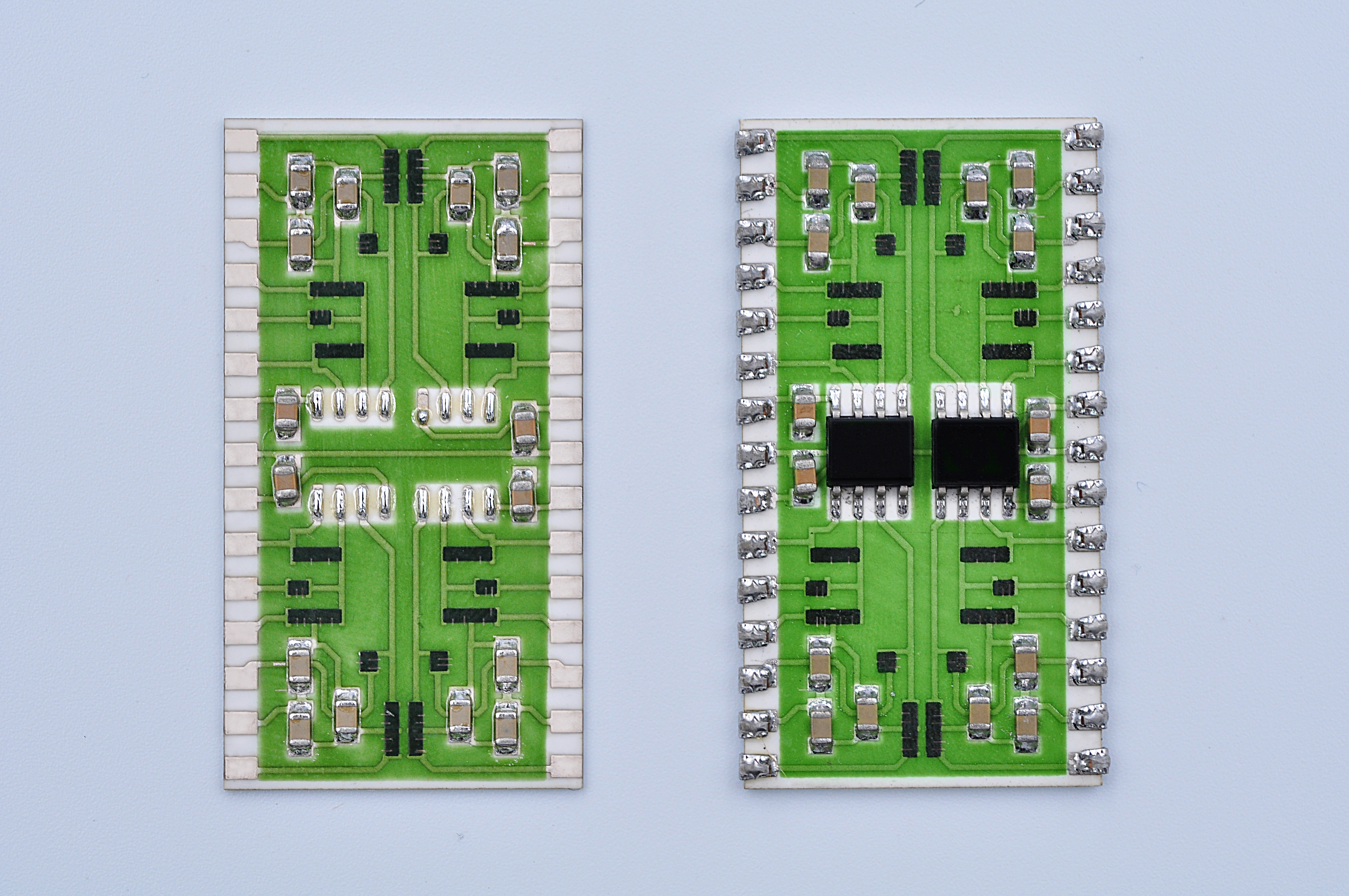
It is supposed that we are familiar with both aluminum PCB and ceramic PCB. But if juxtaposing them, which one will be better by one tally? So, we are about to talk about some differences between them in terms of structure.

Aluminum PCB

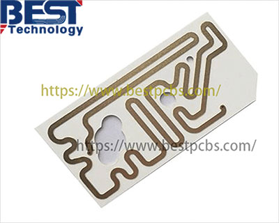
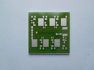
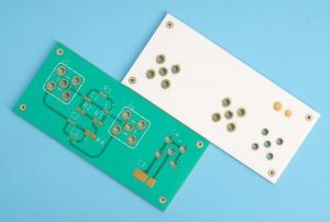
Aluminum substrate namely uses aluminum as substrate, which has a good heat dissipation capacity. Generally, it is single-sided, and also can be double-sided while multi-layer aluminum PCB is a little bit hard to manufacture. Besides, a single layer aluminum PCB is made up of copper layer, dielectric layer and aluminum layer.

Structure of Aluminum PCB

Ceramic PCB

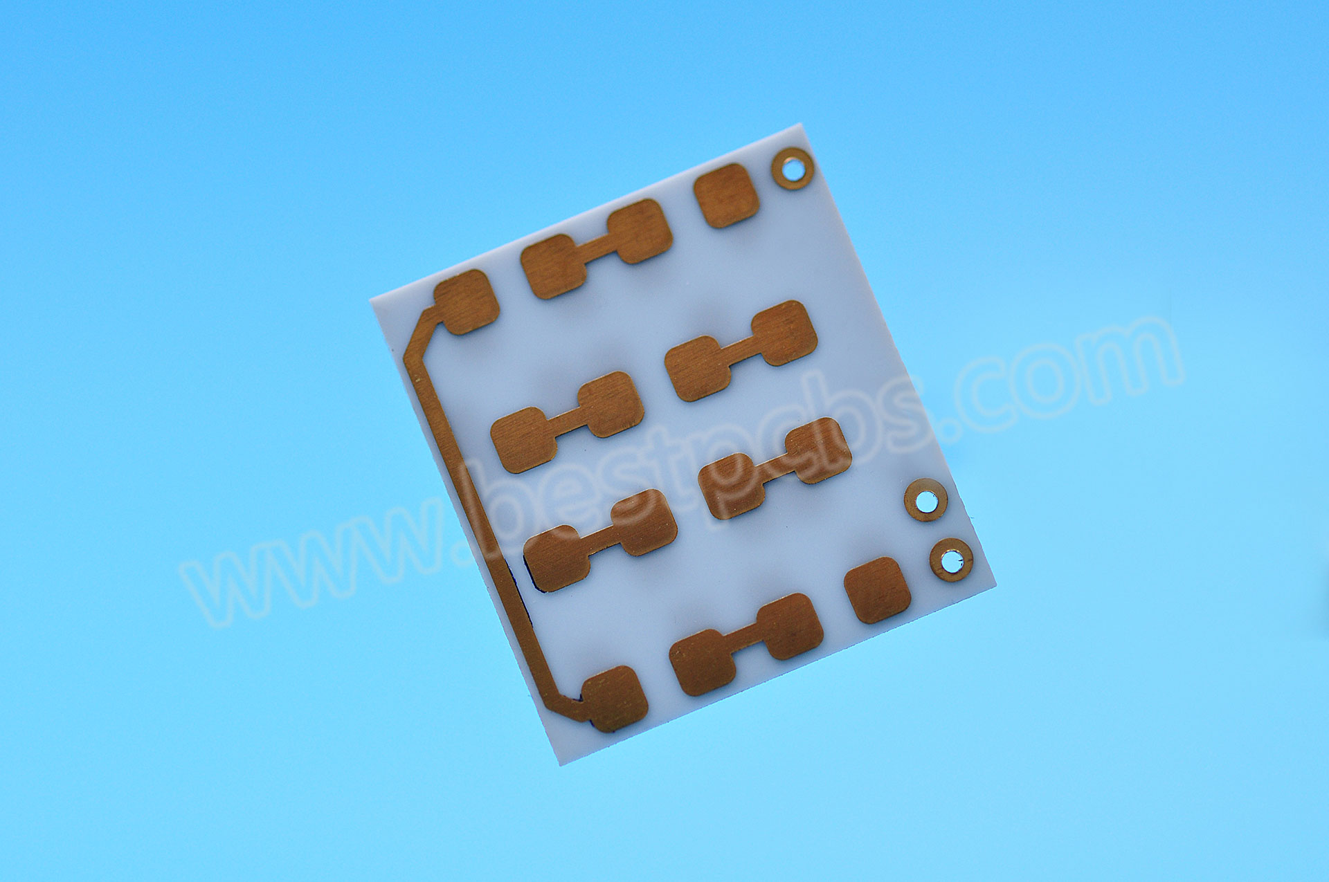
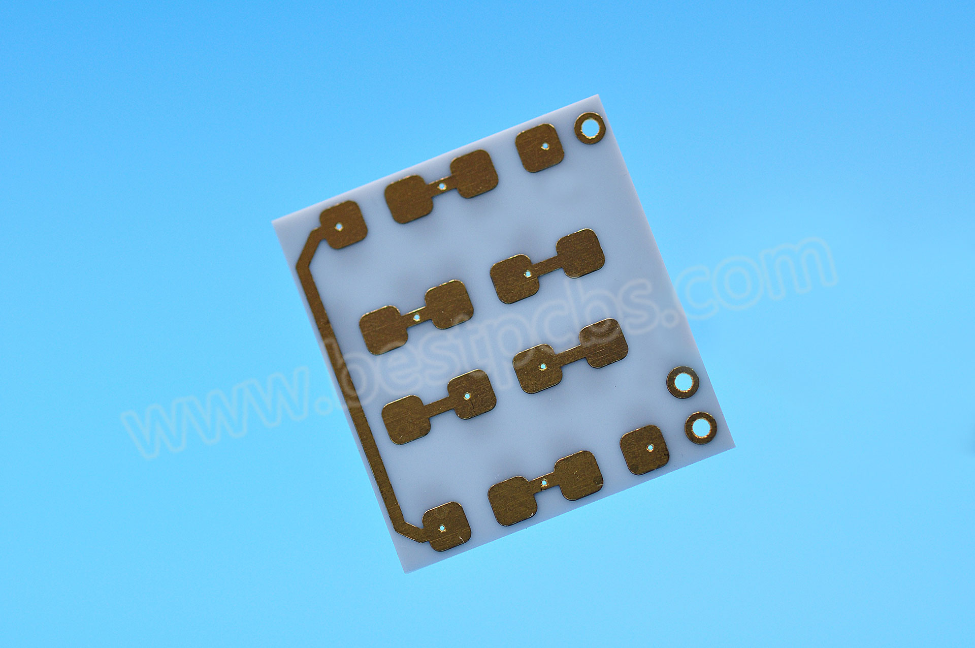
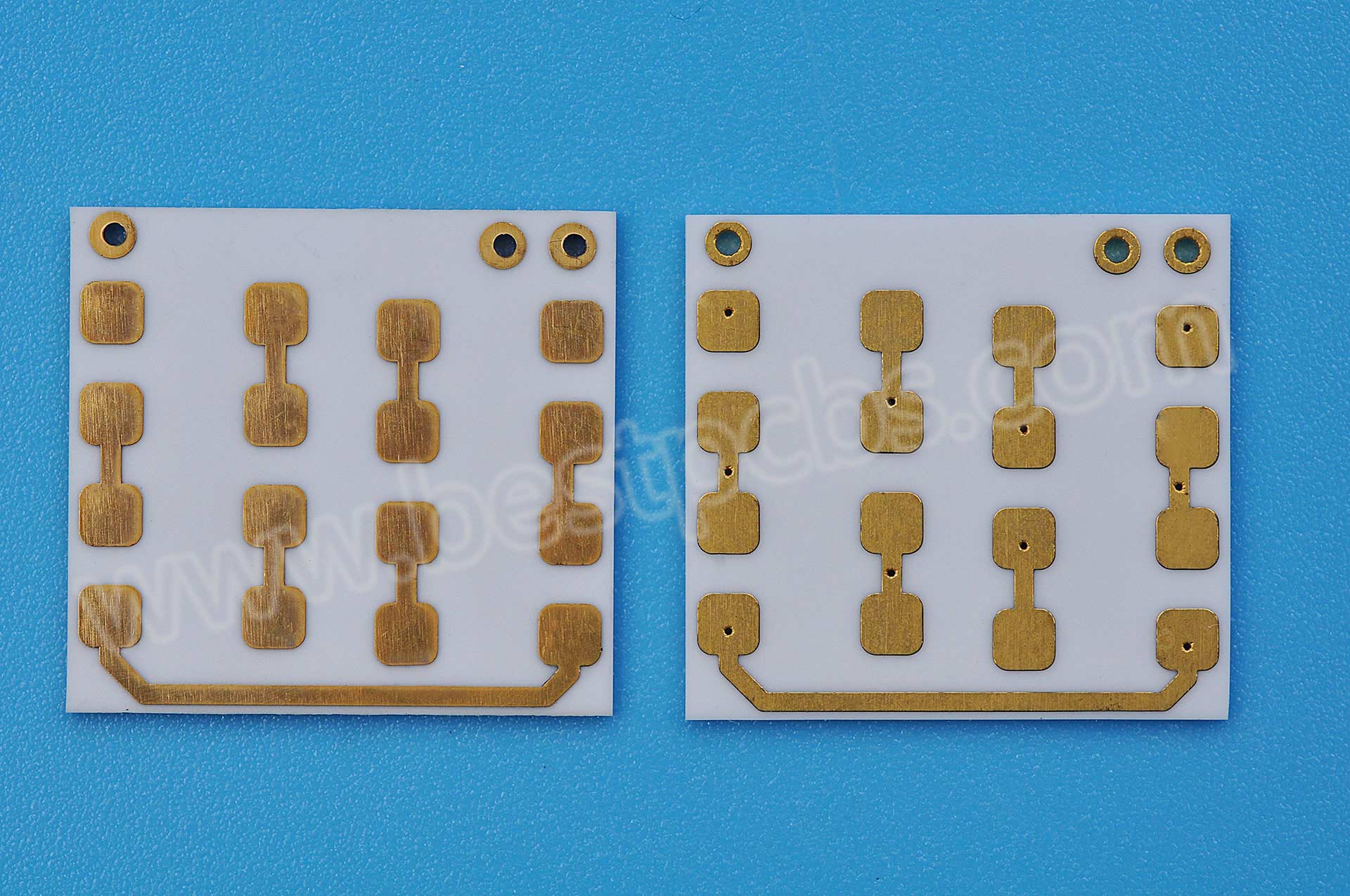
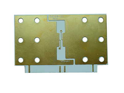
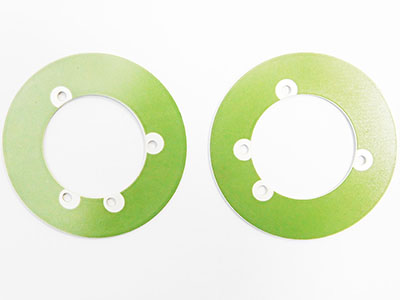
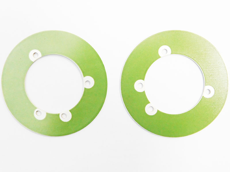
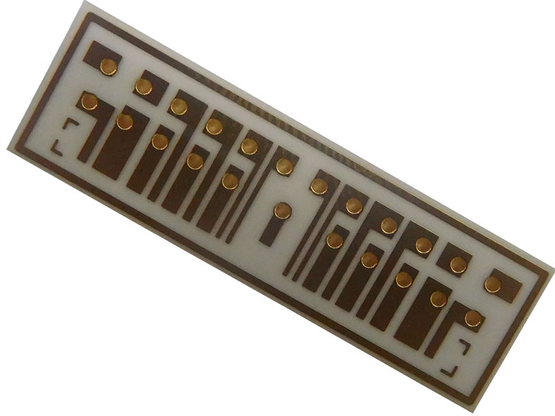
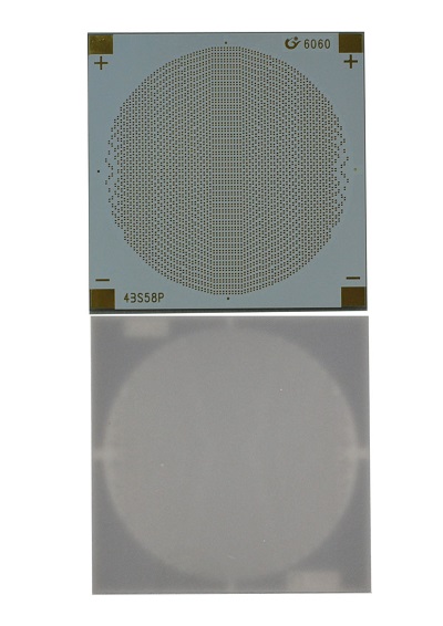
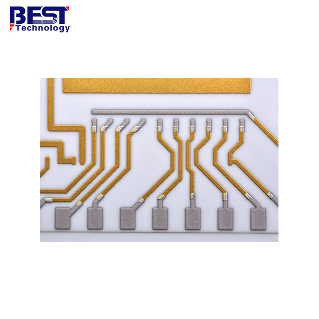
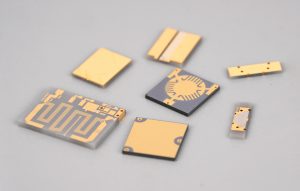
Ceramic PCB namely uses ceramic as substrate. Apart from the material, the structure is the biggest difference between ceramic PCB and aluminum PCB. Since ceramic itself is an insulating material, it does not need a dielectric layer. Its structure is as follows.

Structure of Ceramic PCB

Therefore, whether there is a dielectric layer is the main difference in structure between aluminum PCB and ceramic PCB. And dielectric layer plays an important role in thermal conductivity. So, what is the relationship between dielectric layer and thermal conductivity? And whose thermal conductivity is better between aluminum PCB and ceramic PCB?

We will talk about it next time. And if you would like to know the answer, please feel free to contact us, or you can continuously follow our blog site, we will keep updating more information about the differences between aluminum PCB and ceramic PCB on it.

You may also like

Do the vias can be filled for ceramic PCB?
Friday, November 13th, 2020

As everyone knows for FR4 PCB, people like the vias to be tented or filled for some special applications.
Ceramic PCB is more and more popular because of the thermal conductivity is very high and very good for heat dissipation. Most of customers are going to make the PCB with ceramic material, includes Al2O3, AlN, BeO or Si3N4, etc.
So do the vias can be filled for ceramic PCB becomes the frequently asked questions (FAQ).
The answer is YES.
So what’s the material can be filled in vias for DBC/DPC alumina PCB/ Aluminium Nitride PCB?

The material can be solder mask, Dow Corning 1-4173 and copper/Cu.
Normally, customers want the vias/holes to be filled with copper.
Because copper can fill the vias very well and it is easier to do and it looks very good. Please see below photo.
The left one with filling with copper, the right one without filling copper

Why you need to fill the vias with copper?
1.Becuase if let the vias open, they will allow solder to flow through to opposite side of PCB during reflow, this causes bridging under components.
Filling the open vias/holes with copper can prevent from the solder pates into the vias.
2.If you need to pull vacuum around them and a hole would compromise that, so need to fill the vias.
There are also other purposes for filling the vias, if you need such ceramic board with filling the vias, please contact Coco in Best Technology sales@bestpcbs.com

You may also like

What’s the advantages for AMB ceramic PCB comparing with DPC, DCB, LTCC, HTCC, thick film ceramic PCB?
Tuesday, August 18th, 2020

As we know, there are all kinds of ceramic PCB, DPC ceramic PCB, DBC ceramic PCB, LTCC ceramic PCB, HTCC ceramic PCB, thick film/thin film ceramic PCB.

Very few people know that there is AMB (Active Metal Bonding) ceramic PCB.

Do you know what’s the advantage for AMB ceramic PCB compare with other ceramic PCB (Al2O3/AlN/BeO/Si3N4 PCB)?

For AMB PCB, the substrate can be AlN ( Aluminium Nitride) and Si3N4 (Silicon Nitride) normally, AlN is the most popular. It is widely known that AlN with very high thermal conductivity ( Theoretical Value is 320W/m.k).

Using AMB technology to combine the oxygen-free copper and AlN material under high temperature, AlN with smaller thermal resistance, lower coefficient of thermal expansion and more stable partial discharge capability.

Compared with the traditional DBC or other substrate, the Aluminum Nitride copper-clad ceramic substrate made by the AMB technology with higher bonding strength of the copper layer and better cold and hot cycling characteristics.

So it  is widely used in the field of IGBT, especially for the high-power device control module.

AMB with competitive price and the copper thickness can be much thicker.

AlN max 300um
Si3N4 max 1200um

For more details, please contact me sales@bestpcbs.com 
I will update the manufacture process at the end of this month.

You may also like

Why don’t use BeO as substrate to make DBC ceramic PCB?
Monday, June 22nd, 2020

It is widely known that BeO with high thermal conductivity (200-250W/m.k). High dielectric constant 6-7 (0.1MHz) and dielectric loss tangent is 10-4 (0.1GHz), extremely high working temprature. It is ideal material for ceramic PCB, lots of engineers want to use it as DBC ceramic PCB substrate.

But it is not popular in ceramic PCB market, comparing with Al2O3, AIN, Si3N4, or ZrO2, as the powder of BeO is extremely poisonous.

The poison gas is produced by the reaction between oxygen, Cu and BeO under 1065-1085 degrees Celsius, so it is limited to make cooper on BeO substrate, it has caused ALN (Aluminium Nitride) is becoming more and more popular.

Right now, only few countries are using BeO to make ceramic PCB, such as USA, Russia and China. USA had biggest capability to make BeO , and here in China, there’re still some companies to make BeO raw material and among them, a few companies to produce direct copper bonded (DCB) on BeO because of environment limitation.

Though BeO is not popular for DBC technology, but it is feasible for thick film technology, because when the mentalization of Ceramic PCB, the conductor (Au or AgPd) on BeO substrate was made by silk-screen printing, and drying temperature is only around 850C, no need to under high temperature environment, so there is no chemical reactions, no environment issue.

Below the thick film ceramic PCB manufacturing process for your reference.

https://www.bestpcbs.com/products/thick-film-ceramic-pcb-manufacturing-process.htm

Here is the photo of BeO with AgPd conductor.

BeO with AgPd conductor

Welcome to contact us if you have better idea, or different comments on BeO ceramic PCB, communation will make us becoming better and better.

You may also like

Ceramic Multilayer PCBs: Advantages and Disadvantages
Monday, January 6th, 2020

The primary advantage of ceramic multilayer PCBs lies in their thermal properties. The most significant of these is thermal conductivity, which outperforms traditional materials by a tremendous margin. In the table below, the most used board material, FR4, is compared with the ceramic multilayer board in a number of important categories.

ceramic pcb
ceramic pcb

MULTILAYER PCB MATERIAL COMPARISON

CeramicVersusFR4
28 – 280Thermal Conductivity (Wm-K)0.8 – 1.1
Component ComparableCoefficient of Thermal Expansion (CTE)Component Comparable
HighFrequency PerformanceLow – Mid
FragileHandlingEasy
LowAvailabilityHigh
Mid – HighCostLow – Mid

As shown above, ceramic multilayer PCBs have advantages and disadvantages as compared to FR4. However, the advantages point to a continued increase in the use of ceramic boards for high-speed and high-power applications that are criteria for more functionality in smaller packages.

ceramic pcb
ceramic pcb

Best Technology, the industry leader in fast, precision and high-quality PCB manufacturing, has a wide range of material options including to meet your design objectives. This includes accommodating the special process of using ceramic materials for your board if desired. We also strive to provide you with the best manufacturing experience.

Best Technology’s Custom PCB Manufacturing Service

1.ISO-9001commitment to quality certifications.

2.Accurate quote in less than 1 day.

3.Performs entire turnkey process in as fast as 3 days.

4.Sources components from the most reputable suppliers in the industry to reduce procurement time.

5.Performs multiple automated inspections during assembly to ensure PCB quality for prototyping.

6.Provides support throughout the PCB manufacturing process, beginning with design.

7.Smooth transition from prototyping to production.

You may also like

Fantastic Banquet in Best Technology
Saturday, January 19th, 2019

All works and no play makes Jack a doll. All the guys of Best Technology have worked hard in 2018. In order to reward the members who worked really hard, we had a fantastic banquet on January 18, 2019.

At 7 PM, all the staffs attended the party and the party kicked off with the cheering and applaud. To begin with, our general manager Peter gave a speech which showed the conclusion of 2018 and his ambition for 2019.

Peter gave a speech

Peter gave a speech

After the speech finished, we began to reward the staff one by one. Compared with the ceramic PCB, FR4 PCB and metal dome, the flex circuits got the first place. Mrs Celine won the sales champion of flexible PCB.

Celin won the champion of sales

Celin won the champion of sales

Compared with last year, we have more entertainment programs in the banquet of 2018. Dancing, singing and games, all of these programs made us feel relax and forgot the pressure of work.

Dacing

Dacing

What a fantastic banquet we had. Time flies, the beautiful night quickly came to an end and we took a family picture to remember this party.

Family picture

Family picture

2018 has gone, and we will hold hands and work together to achieve the gold of 2019. since throwing his hat into printed circuit board, Best Technology is always dedicated to uphold our mission:to provide the most suitable products and the most satisfying service for our customers. If any interested in rigid PCB, rigid-flex PCB or ceramic PCB, please feel free to contact us at sales@bestpcbs.com or call us at 0755-29091601.

You may also like

The Application of Ceramic PCB in Communication Industry
Wednesday, January 16th, 2019

Time goes by, the communication of human being still reforms constantly. We are surrounded by various of communication tools, including broadcasting, mobile phone, GPS etc.. And they have become an indispensable part in our daily life. The reason why they are able to serve for us is not only depend on the development of science, but also benefit from a kind of media–antenna. Antenna is the key to the communication. If there is a problem, the connection of signals will be lost.

The antenna can be used in various environments, so it is difficult to meet the requirements of itself. In order to ensure that the antenna can work normally, it is necessary to ensure its quality, whether in the selection of material or in the production process.

Ceramic PCB

Ceramic PCB

The common printed circuit board can not meet the performances of the antenna. Nowadays, the most suitable product is the ceramic PCB. The ceramic PCB possesses various benefits as following:

  1. The dielectric constant is small.
  2. Low loss in high frequency.
  3. Having good performance in signal transmission.
  4. High boding strength between metal layer and the substrate of the ceramic PCB.
  5. With good performance in insulation. It will appear high voltage during the antenna is working, but it is incredible dangerous for human being. The ceramic PCBhas nice performance in insulation and the resistance in breakdown voltage is up to 20KV/mm which is able to protect human safety effectively.
  6. It can be used in high density assembly. The line space resolution of the ceramic PCBis able to reach 20μm, so that the lightness and thinness of the communication equipments can be realize.

Ceramic PCB

Thick film ceramic PCB

As a professional printed circuit board in China, Best Technology is always dedicated to catch up with the development of times to fabricate ceramic printed circuit boards with high quality. Withe the development of communication, we would love to provide products that offer a competitive supply of thick film  ceramic PCB and thin film ceramic PCB and other ceramic PCB products. To find out more information, contact Best Technology at 0755-29091601 or check the website: https://www.bestpcbs.com

You may also like

Xiaomi Integrated IKEA’s Smart Lighting Products in IoT Platform
Friday, December 7th, 2018

Xiaomi co-founder and CEO Lei Jun said,“To connect everything needs collaboration with others.â€ÂOn November, 2018, Xiaomi announced a strategic partnership with IKEA. IKEA’s full range of smart lighting products will be connected to Xiaomi’s IoT platform starting this December in China. This marks the first time IKEA has partnered with a Chinese technology company.

Through the cooperation, the lighting products of IKEA can be controlled by smart speakers including Xiaomi’s AI voice assistant Xiao Ai, which is currently only available for Chinese Mandarin speakers.

Most of Xiaomi’s fans might know that its ‘Mi Home’ app designed to manage Xiaomi devices and products as well as Xiao Ai will be compatible in IKEA’s smart lighting products.

Speaking at the Xiaomi AIOT Developers Conference, Lei Jun said the combination of artificial intelligence (AI) and IoT will be the core strategy of his company’s business in ten years.

Fan Dian, General Manager of the IoT platform department of Xiaomi, said, “IKEA and Xiaomi share very similar values and I believe our collaboration will accelerate the development of the smart home industry across the world.â€Â

According to the company’s third-quarter financial report, Xiaomi has connected 132 million IoT devices in the ended September.

With a goal to allow people to fully embrace AI in daily life at home, more and more PCBs are applied into connected home. Because the benefits of high thermal conductivity and heat dissipation highly meet the requirements of the market, the aluminum core PCB and ceramic PCB are the perfect match for LED lights. If you would like to add more colors for your smart home, the aluminum core PCB and ceramic PCB from Best Technology are nice choice.

You may also like

What the Maximum Current the Thick Film Ceramic PCB can be Carried?
Tuesday, January 27th, 2015

A lot of customers ask us what the biggest current his circuit can be carried, or how can I got a 6 Amps trace? We believe most of engineer design the thick film ceramic PCB, he will consider that, so we share information bellowing and hope it’ll be helpful for you.

When you try to know current, you also need to know the watts of trace will be, and then need to know the power density of thick film ceramic PCB firstly. The power density for conductor itself should be limited to max 600 Watt/inch2 of conductor surface. And power density for an Al2O3 substrate should be limited to 8 Watts/in2 (for the total of all conductors on top of it).

If you have a Ag conductor line of 0.3inch long, 0.010 inch wide (=30 square (0.3/0.01)), the surface area is 0.3 x 0.01 = 0.003 in2. This means the carrying powder P is limited to 600 (power density) x 0.003 (area) = 1.8 watts.

Assume conductor resistivity is 6mOhm/sq/12.5um (material P/N: ESL9562), the resistance value R = 30 sq x 6mOhm = 0.18 ohm.

Power = I2 x R, or I2 =Power/R=1.8/0.18 = 10, so the carrying current limit I = 3.16 amps. Or in a short equation,

I (amps) = line width (inch) x (power density)1/2 / (sheet resistance, ohm) 1/2

  1. If the trace keep 0.3 inch long, but change width to 0.02inch, (=15 square (0.3/0.02), the surface area is 0.3 x 0.02 = 0.006 in2. This means the carrying powder P is limited to 600 (power density) x 0.006 (area) = 6 watts.
    And resistance value for that trace will be 15 square x 6mOhm = 0.09 ohm, and then 3.6/0.09= 40, I=6.325 amps.
  2. If the trace width keep 0.01inch, but change line to 0.6 inch long (=60 square (0.6/0.01), the surface area is 0.6 x 0.01 = 0.006 in2. This means the carrying powder P is the same as 6 watts. (600×0.006).
    But the resistance value for that trace will change to be 60 square x 6mOhm = 0.36 ohm, and then 3.6/0.36= 10, I=3.16 amps. So you can see, it’s no useful to change the trace line.

So if you want to have bigger current for thick film ceramic PCB, then you need to increase the width of trace.

Hope above is clear for everybody. Please leave your comments on that power density of thick film ceramic PCB.

You may also like

Bigger size of Ceramic PCB is Available Now!
Wednesday, December 10th, 2014

Good news! This month we have used a new machine which can print much bigger size of silver palladium, Gold palladium, and glass glaze on Thick Film Ceramic PCB.

Currently the normal dimension in thick film Ceramic PCB is about 80 x 138mm and that size has already limited a lot of designs. You can’t put too much trace, PAD on such smaller size board, and the you have to use 2 layer, or 4 layers ceramic board to put more trace. And of course, that will increase a lot of cost definitely!

Now, we can make 200 x 200mm (8×8 inch). Thinking about the normal 80x138mm and you will find out this is an extreme improving! See bellowing pictures show the comparing!

Ceramic PCB size comparing

Ceramic PCB size comparing

So now you don’t need to worry about the size! You can design as big as you want!

And we are also continuing to adopt first-of-art machine and technology to make bigger size, higher quality Ceramic PCB!

Please contact us if you have more good idea, or suggestion about Ceramic PCB.


You may also like