Are you interested in power LED PCB and how to design a high power LED PCB board? Let’s learn more about types, advantages of power LED PCB and how to design high power LED PCB for better dissipation through this blog.
Best Technology, we focus on power LED PCB design service over 18 years. And we deliver high-performance Power LED PCBs with free technical support, multi-engineer collaboration, and cost-saving DFM analysis to optimize designs and reduce production cost. Rigorous in-house EMC testing ensures compliance (FCC/CE), while rapid prototyping (<7 days) and ISO 9001/RoHS/UL-certified manufacturing guarantee reliability. Leverage our expertise in thermal management, custom substrates (aluminum/ceramic), and eco-friendly practices to cut costs and accelerate your project. If you have any request for power LED PCB, please contact us: sales@bestpcbs.com
What Is Power LED PCB?
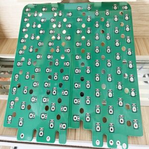
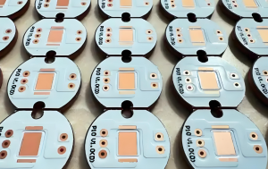
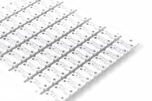
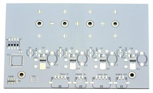
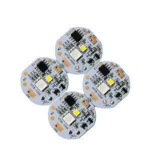
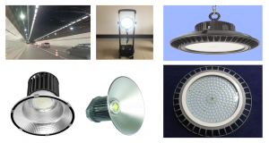
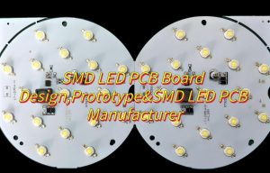
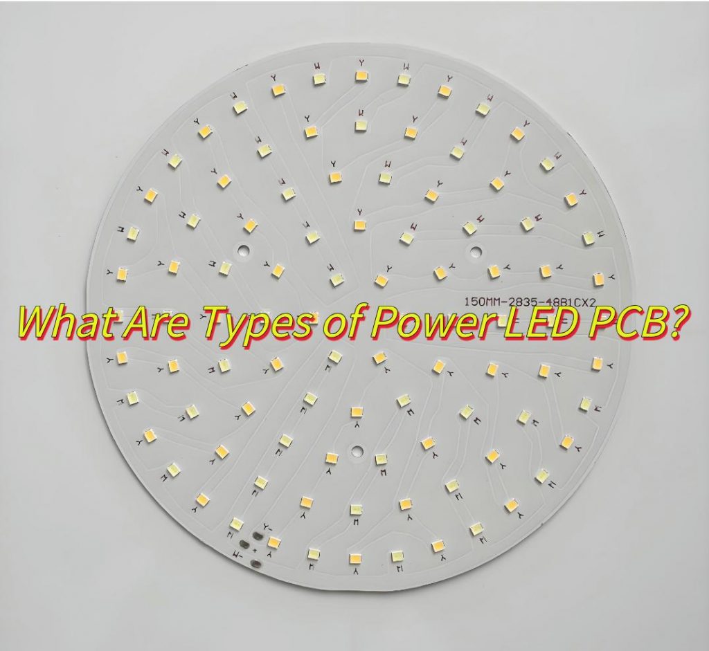
Power LED PCB is a printed circuit board designed for high power LEDs.(like high power 3535 LED PCB and high power 5050 LED PCB). It uses a metal substrate (such as aluminum) and a special thermal conductive structure to achieve efficient heat dissipation. It ensures stable transmission of large currents by widening copper foil routing and optimizing pad layout. It is widely used in high-intensity solid-state lighting systems such as industrial lighting and car lights.
What Are Types of Power LED PCB?
Types of Power LED PCBs:
- Metal-Core PCB (MCPCB)-Aluminum or copper substrates with insulated thermal layers for high-power LED lighting such as streetlights and automotive headlights, like power LED aluminum PCB.
- Heavy Copper PCB-Thick copper traces (≥3 oz/ft²) for high-current applications like LED driver circuits and industrial power modules.
- Multi-Layer PCB-4+ conductive layers with thermal vias and EMI shielding for LED displays, automotive electronics.
- High-Frequency PCB-Low-loss materials (e.g., PTFE) for stable signal transmission in 5G/RF lighting and radar systems.
- Rigid-Flex PCB-Hybrid design combining rigid stability and flexible routing for automotive lighting.
What Are Advantages of LED Power PCB?
Advantages of LED Power PCBs:
- Efficient thermal management ensures optimal heat dissipation, prolonging LED lifespan.
- High energy efficiency with minimal power loss due to low-resistance circuitry.
- Compact design enables integration into space-constrained applications.
- Enhanced durability with robust materials resistant to vibration, moisture, and temperature fluctuations.
- Precise current regulation improves LED performance and brightness consistency.
- Eco-friendly operation with low power consumption and reduced carbon footprint.
- Customizable layouts support complex circuit designs for diverse LED applications.
- Cost-effective production through scalable manufacturing and reduced maintenance needs.
Why Choose Aluminum for Power LED PCB?
Reasons for why choose aluminum for power LED:
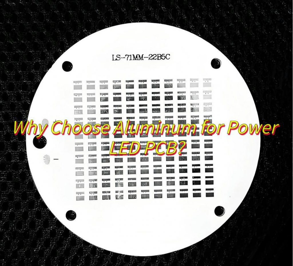
- Efficient Heat Dissipation: High thermal conductivity prevents overheating, extending LED lifespan.
- Durability: Resists thermal stress, vibration, and maintains precise dimensions.
- Electrical Reliability: Handles higher currents, blocks interference, and ensures insulation.
- Cost-Saving: Recyclable material, reduces heatsink needs, and lowers bulk production costs.
- Custom Design: Adapts to complex shapes and multi-color LED configurations.
How to Design 3W Power LED PCBs for Brightness?
This is how to make 3w power LED PCB design for brightness:
1.Thermal-Centric Substrate Design
- Use 2.0mm aluminum MCPCB with dielectric layer thermal conductivity ≥3.0 W/mK.
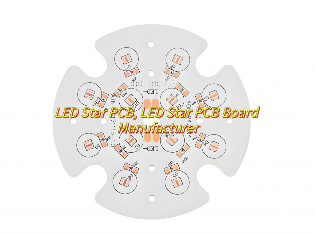
- Design star-shaped LED placement (4 LEDs total) with 8mm spacing to isolate heat sources.
2.Constant-Current Circuit Implementation
- Integrate buck driver (e.g., TI LM3409) set to 700mA ±2% with feedback resistors (0.7Ω/1%).
- Add PWM dimming circuit (100–1k Hz) using MOSFET and microcontroller (e.g., STM32) for brightness adjustment.
3.Copper Layout Optimization
- Apply 3W rule: Trace spacing ≥3× trace width (e.g., 2mm traces with 6mm spacing).
- Use 2oz copper thickness for power traces and widen ground planes to reduce resistance.
4.Thermal Management Execution
- Drill thermal vias (0.4mm diameter) under LED pads, filled with conductive epoxy (≥4 W/mK).
- Attach extruded aluminum heatsink (30×30×15mm) using thermal tape (3.5 W/mK).
5.Optical Enhancement
- Apply 98% reflective white solder mask around LEDs and use 45° angled sidewalls to maximize light output.
- Embed diffuser layer (PC material) in the final assembly to homogenize brightness.
6.Prototyping & Testing
- Measure luminous flux with integrating sphere, calibrate PWM duty cycle to achieve ±3% brightness uniformity.
7. EMI/EMC Compliance
- Add π-type filters (10µF ceramic + 10µH inductor) at driver input/output to suppress noise.
- Test radiated emissions per FCC Part 15B using near-field probes.
8.Production Readiness
- Generate Gerber files with 0.2mm solder mask dam and 0.15mm solder paste stencil.
- Validate assembly process with 3D STEP model to check component clearance.
How to Balance Current in High Power LED PCB Layouts?
To balance current in high power LED PCB layouts:
Symmetrical Star-Shaped Routing
- Arrange LEDs in a radial pattern with equal-length traces radiating from a central power node. This minimizes impedance differences between parallel branches, ensuring even current distribution.
- Use identical trace widths and spacing for all parallel paths to eliminate resistance variations.
Thick Copper Layers (≥3 oz/ft²)
- Increase copper thickness to reduce resistive losses in high-current paths. For example, 3 oz/ft² copper handles up to 6A/mm trace width (vs. 3A/mm for 1 oz/ft²).
- Prioritize short, direct traces to minimize voltage drops.
Thermal Symmetry
- Align PCB thermal management structures (e.g., heat sinks, thermal vias) symmetrically around LEDs to maintain uniform junction temperatures.
- Avoid placing high-power components near PCB edges, which can create thermal gradients.
Parameter Matching
- Use LEDs from the same production batch to minimize forward voltage and current tolerance variations (ideally <2% mismatch).
- Group LEDs with similar electrical characteristics into parallel clusters.
Low-Impedance Grounding
- Design a solid ground plane beneath power traces to stabilize return paths and reduce EMI-induced current fluctuations.
- Place decoupling capacitors near LED nodes to suppress transient noise.
Active Current Regulation
- Integrate current-sharing resistors (e.g., 0.1Ω–0.5Ω) in series with each LED branch to compensate for minor mismatches.
- For precision control, use dedicated LED driver ICs with built-in current balancing (e.g., TLC5916, LT3763).
How to Route High Power LED PCB Lines Cheaply?
To route high power LED PCB lines cheaply:
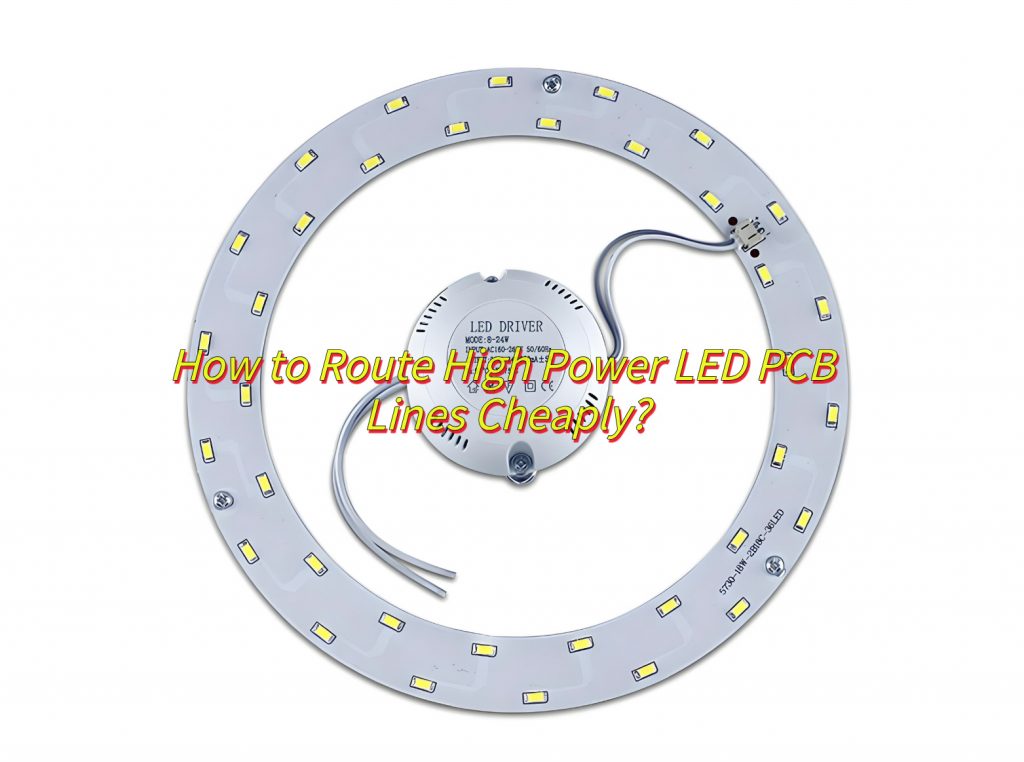
- Prioritize single/double-layer PCB designs with 2oz copper thickness for current capacity, using FR4 substrates instead of metal-core boards. Integrate 12–24 thermal vias (0.3mm diameter) per LED and attach extruded aluminum heatsinks (cost ≤$0.10/cm²) for thermal management.
- Follow the 3W spacing rule: Maintain ≥3× trace width between conductors (e.g., 0.6mm spacing for 0.2mm traces) to reduce interference. Add 1mm isolation zones for critical signals like clocks or high-speed lines.
- Cluster components (LEDs, drivers, capacitors) within 15mm radius: Use star topology for power routing (<30mm trace length) and implement solid ground planes with multi-point connections (impedance below 5mΩ).
- Match trace widths to current loads using PCB current calculators. Use tapered traces to minimize current spikes and avoid excessive temperature rise.
- Simplify driver circuits: Use linear ICs (e.g., AMC7135) with 1% current-limiting resistors for <2A applications. For >2A, adopt discrete MOSFET solutions to cut costs by 40% compared to integrated ICs.
Can Multi-Layer Designs Solve High Power LED PCB Overheating?
Yes, multi-layer design can effectively alleviate the overheating issue of high power LED PCBs. By embedding a thick copper layer (≥2 oz) as a heat dissipation layer and combining vertical thermal vias (0.3–0.5mm) to quickly guide heat to the radiator, the symmetrical stacking structure and high temperature substrate (such as aluminum baseboard) can disperse thermal stress. In conjunction with active cooling measures (such as thermal interface materials), it is possible to control the junction temperature within a safe range (<85°C). However, it is necessary to plan the thermal path and electrical isolation reasonably to avoid thermal coupling failure.
In conclusion, that’s all about power LED PCB and how to design a high power LED PCB board for better dissipation. If you have any other issues for power LED PCB and high power LED PCB, welcome to leave a message below this blog.


