pcb
Home > Blog

Posts Tagged ‘PCBA’

What is the surface mount technology?
Friday, August 23rd, 2024

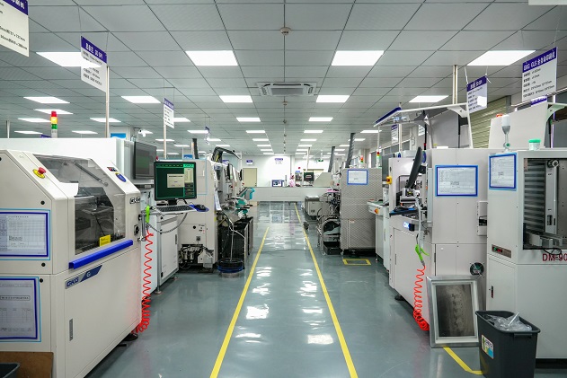
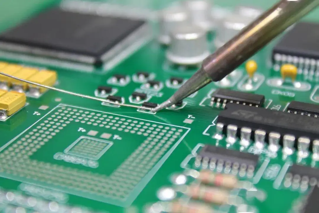
Surface mount technology (SMT) is a widely used surface assembly method in the electronic assembly industry. It mainly uses automated production equipment to directly solder surface mount components (SMD) to the pads on the surface of the printed circuit board (PCB). SMT has the advantages of high production efficiency, high space utilization, high density and miniaturization. However, it has high requirements for production equipment, processes and operating skills.

What is the surface mount technology process?

The process of surface mount technology (SMT) mainly includes the following steps:

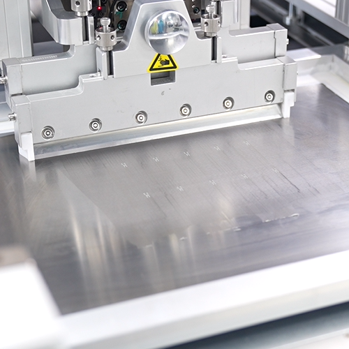
1. Printed circuit board preparation: Before surface mounting, the printed circuit board needs to be prepared first, including cleaning the circuit board, removing the surface oxide layer, and applying solder paste.
What is the surface mount technology ?

2. Component mounting: Use appropriate equipment to accurately mount various electronic components on the printed circuit board.

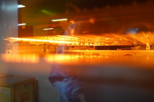
3. Soldering: After the components are mounted, the solder paste is heated to melt it to form a reliable welding connection.

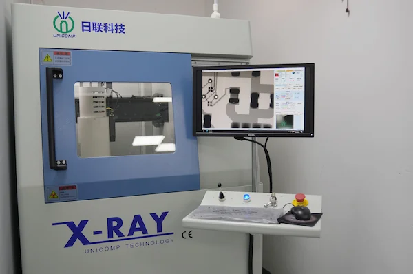
4. Inspection: After welding, use AOI for automatic inspection to ensure the correct mounting and welding quality of components.

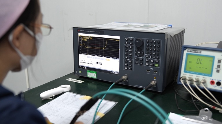
5. Testing and debugging: Test and debug the mounted circuit board, and verify whether the function and performance of the circuit board meet the requirements through specific test equipment and procedures.

Each step needs to be carried out carefully to ensure that the mounted circuit board has good quality and reliability. In addition, surface mount technology is suitable for circuit board assembly, with the characteristics of compact structure and small size, and is widely used in the manufacture of electronic products.

What are the roles of surface mount?

The role of surface mount technology (SMT) is mainly reflected in improving the performance, reliability and production efficiency of electronic products, while reducing the volume and weight of products.

Surface mount technology (SMT) has the following significant effects:

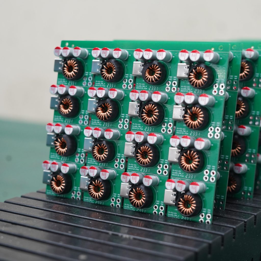
Increase assembly density and reduce product volume: By using surface mount technology, the volume of electronic products can be reduced by 40%~60% and the weight can be reduced by 60%~80%.
What is the surface mount technology ?

‌Improve reliability: SMT has high reliability, low solder joint defect rate and strong vibration resistance.

Optimize high-frequency characteristics: SMT reduces electromagnetic and radio frequency interference and optimizes the high-frequency characteristics of the circuit.

Automated production: SMT is easy to automate, thereby improving production efficiency.

Enhanced compactness: Using small surface-mounted components can save a lot of space on the printed circuit board, and circuit assembly is easier to automate.

Adapt to a wide range of fields: As a new generation of electronic assembly technology, SMT has penetrated into various fields, including but not limited to computers, communication equipment, consumer electronics, etc.

In summary, surface mounting technology has significantly improved the comprehensive performance and production efficiency of modern electronic products by increasing assembly density, optimizing circuit performance, enhancing product reliability, and realizing automated production.

What is the advantage of surface mount?

The advantages of surface mounting mainly include:

High assembly density: Surface mounting technology (SMT) allows more electronic components to be installed in a limited space.

Small size and light weight of electronic products: By using SMT, smaller and lighter electronic products can be manufactured.

‌High reliability‌: SMT has a low solder joint defect rate, which improves the reliability of the product‌.

‌Easy to automate‌: SMT technology is very suitable for automated production and can greatly improve production efficiency‌.

‌Design flexibility‌: SMT allows different components to be used on the same circuit board, providing design flexibility‌.

‌EMC compliance‌: SMT technology helps meet electromagnetic compatibility (EMC) requirements and ensure the safety and performance of the equipment‌.

‌Selective soldering‌: SMT supports selective soldering, which increases the customizability of the product‌.

In addition, SMT technology is cost-effective because the packaging size of components is generally standardized and can be quickly and accurately installed using automated equipment, thereby reducing production costs‌. At the same time, SMT reduces human errors and improves product quality because the placement of components is very consistent, reducing errors or the need for rework.

What are the disadvantages of surface mount?

‌The disadvantages of surface mount technology (SMT) mainly include incompatibility with certain components, the possibility of soldering defects, and high equipment costs. ‌

‌Incompatibility with certain components‌: SMT technology is not suitable for all types of components.

‌Possibility of soldering defects‌: Although SMT technology reduces the need for drilling and shortens setup time, it is not a zero-defect soldering process. In actual applications, SMT may encounter various soldering defects.

‌Higher equipment cost‌: Although SMT technology can improve production efficiency and circuit density, it requires expensive special equipment and professional technicians.

In summary, although SMT technology has many advantages, such as reducing drilling, shortening setup time, and improving production efficiency, it also has some disadvantages, especially in terms of incompatibility with certain components, possible soldering defects, and high equipment costs.

What does SMD stand for in surface mount?

SMD stands for Surface Mounted Devices. ‌

SMD is a type of component in surface mount technology (SMT), which is characterized by small size, high power, stable performance, and easy automated assembly.
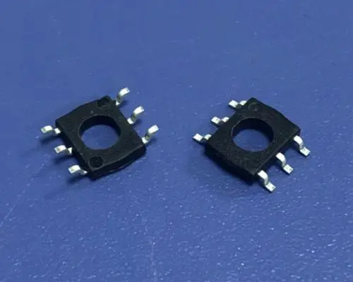
What is the surface mount technology ?

SMD packaging technology can maximize the space utilization on the circuit board, especially for the design of dense circuit boards. SMD packaging usually adopts metal oxide semiconductor (MOS) technology, and its packaging methods are diverse, including COB, QFN, LCC, BGA, etc.

In practical applications, the appearance inspection of SMD devices includes visual inspection or use of a magnifying glass to check whether the solder end or pin surface is oxidized or has contaminants, and to ensure that the nominal value, specification, model, accuracy, and external dimensions of the components are consistent with the product process requirements. To ensure the performance and reliability of the device.

The wide application of SMD technology not only improves the performance of electronic products, but also promotes the automation and efficiency improvement of the electronics manufacturing industry. It is an indispensable part of the modern electronics manufacturing industry, especially in applications that require high integration and high reliability.

What is the application of surface mount?

The application of surface mount technology is mainly reflected in improving production efficiency, reducing product volume and weight, and meeting the market demand for miniaturized, lightweight, and high-performance electronic products. This technology is mainly used to mount electronic components on printed circuit boards (PCBs) to achieve circuit connection and system integration.

Surface mount technology can replace traditional through-hole insertion technology, thereby improving product reliability and performance and reducing costs. The technology has a wide range of applications, including but not limited to consumer electronics, military cutting-edge electronics, and fire detectors, manual alarms, and various electronic modules.

In the manufacture of electronic products, surface mount technology has become a revolutionary change, dominating the development of electronic equipment and bringing about major changes in electronic products.

Conclusion:

Usually, the electronic products we use are designed by PCB plus various capacitors, resistors and other electronic components according to the designed circuit diagram, so most electrical appliances require various SMT (patch) processing technologies to process.

BEST Technology focuses on the procurement and processing of various electronic products and processing services for incoming materials, including but not limited to SMT patches, DIP plug-ins, welding, functional testing and maintenance, and assembly proofing and batch production. We can provide proofing, small batch and batch SMT mounting, and can also purchase electronic components and make PCBs.

You may also like

What is a PCB assembly?
Thursday, August 22nd, 2024

PCB assembly is the process of combining a circuit board with other electronic components (such as connectors, housings, heat sinks, etc.) to embed into a final product. This process is a key step in the production of electronic equipment. Its main function is to provide a platform for electronic components to work together in a coordinated manner so that the equipment can perform its intended tasks.

What is the standard for PCB assembly?

The standards for PCB assembly mainly include PCB panel specifications, ISO standards, IPC standards, JEDEC standards, and ROHS standards. ‌

What is a PCB assembly?

‌PCB panel specifications‌ involve the width, shape, frame design, center distance between small boards, setting of positioning holes, arrangement of reference symbols, and positioning of large components of the panel. The panel frame should adopt a closed-loop design to ensure that the panel is fixed on the fixture without deformation.

‌ISO standards‌ emphasize key factors such as fit tolerance, surface roughness, contact area, and tightening force in PCB tight-fit installation to ensure the accuracy and stability of installation‌.

‌IPC standards‌ include IPC-7711 and IPC-A-600E, the former provides basic recommendations and guidelines for the design and manufacture of printed boards, and the latter provides acceptable conditions and practice guidelines for printed boards.

‌JEDEC standards‌ provide specifications for circuit board materials, dimensions, interfaces, etc., including material selection, dimension design, interface specifications, test methods and quality assurance.

‌ROHS standard‌ is a directive on the restriction of the use of hazardous substances, aimed at reducing the impact on the environment and human health. It stipulates the use restrictions of hazardous substances such as lead, mercury, cadmium, hexavalent chromium, polybrominated biphenyls and polybrominated diphenyl ethers.

Compliance with these standards ensures the quality, safety and environmental friendliness of PCB products, and also provides clear guidance and specifications for the design, manufacture and assembly of PCBs.

Why is PCB assembly so expensive?

The high cost of PCB assembly is mainly due to the combined influence of multiple factors. ‌

First, the production cost of PCB boards is affected by materials, design and manufacturing complexity, precision and quality, and supply chain and regional differences. PCB boards are mainly made of materials such as copper, fiberglass and epoxy resin, and the cost of these materials directly affects the price of PCB boards.

The complexity of the design and manufacturing process, including pre-processing, image transfer, electroplating, etching, inspection and trimming, and post-processing, requires precise tools and professional skills, which will also be reflected in the cost. High-precision PCB boards require higher manufacturing costs because they require more precise tools and more stringent manufacturing processes.

Details in the PCB assembly process, layer selection, and the application of HDI technology will all have an impact on the cost. Every small change may cause the cost to plummet, so if you want to save money without losing performance, you need to consider these factors comprehensively.

In addition, the welding process is also a costly link. Soldering is a key step in fixing electronic components to PCBs. This process requires heating each joint separately for welding, which is a slow and laborious process.

Finally, the price of PCBs is also affected by factors such as materials, surface processing, design standards, copper foil thickness, quality acceptance standards, and mold fees and test frames. For example, different materials, surface processing, and copper foil thickness will lead to price differences.

In summary, the high cost of PCB assembly is mainly due to the combined effect of multiple factors such as material cost, manufacturing complexity, precision and quality requirements, production needs, and specific design and quality requirements.

What does PCB stand for?

PCB stands for Printed Circuit Board. ‌

What is a PCB assembly?

Printed circuit board (PCB), also known as printed circuit board, is an indispensable component in electronic engineering. It is the support of electronic components and also the carrier of electrical connection of electronic components.

Printed circuit boards are widely used in various electronic devices. Printed circuit boards can be divided into single-sided boards, double-sided boards, multi-layer boards, etc. according to the number of layers of circuit boards. Among them, multi-layer boards refer to printed boards with more than two layers. It consists of connecting wires on several layers of insulating substrates and pads for assembling and welding electronic components. It has the function of conducting each layer of circuits and insulating each other.

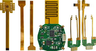
The wide application of printed circuit boards makes it possible to miniaturize and visualize the circuits of electronic devices, which plays an important role in the mass production of fixed circuits and optimizing the layout of electrical appliances. This type of circuit board uses polyimide or polyester film as the substrate, and has the characteristics of high wiring density, light weight, thin thickness and good bendability.

What is the difference between PCB and PCBA?

The main difference between PCB and PCBA lies in their definition, function, application and manufacturing process. ‌

Definition:

PCB (printed circuit board) is a basic electronic component made by electronic printing, mainly used as a support for electronic components, and does not contain any active or passive components.

PCBA (printed circuit board assembly) is a circuit board assembly with specific functions formed by soldering electronic components to PCB through processes such as SMT (surface mount technology) or THT (through-hole mounting technology). PCBA contains PCB and all necessary electronic components, which work together to realize the preset functions of the circuit board.

What is a PCB assembly?

‌Function and application‌:

The main function of PCB is to support and connect electronic components, while PCBA integrates electronic components into a complete circuit system, which can be used in the manufacture of various electronic products.

PCBA is the core part of electronic products and directly determines the performance and function of the product.

‌Manufacturing process‌:

The manufacturing process of PCB includes circuit design, PCB board design, PCB template production, copper foil etching, drilling, tin spraying and board making.

The production of PCBA requires component mounting, welding, testing and other processes.

In summary, the main difference between PCB and PCBA lies in their definition, function, application and manufacturing process. PCB is a basic electronic component, mainly used to support and connect electronic components, while PCBA is a finished product formed by welding electronic components to PCB. It has specific circuit functions and is an indispensable part of electronic products.

What is the difference between PCB manufacturing and assembly?

The main difference between PCB manufacturing and assembly is that they involve different processes and focuses. ‌

‌PCB manufacturing‌ mainly involves the process of converting raw materials into printed circuit boards through a series of process flows, including design, layout, etching, lamination, drilling, welding and other steps, and finally forming a complete and usable printed circuit board.

‌PCB assembly‌ is the process of soldering electronic components to the printed circuit board according to the design requirements after the PCB is manufactured. The focus of assembly is to ensure that all components are in the correct position and direction, the pins of each component are fully soldered to the designated pads, and there is no excess solder or other excess materials to ensure the normal operation and reliability of the circuit board.

In short, ‌manufacturing‌ covers the entire production process from raw materials to finished products, including design, production and testing, while ‌assembly‌ is a link in the manufacturing process that focuses on accurately mounting electronic components on printed circuit boards to ensure the final function and performance of the product.

Conclusion:

PCB assembly is an important part of manufacturing and affects the quality of the final product. Therefore, choosing the right manufacturer becomes particularly important. BEST Technology is committed to becoming the world’s most trusted one-stop electronic circuit solution provider, while focusing on PCBA prototyping and small batch production. Choosing us will get the best quality products.

You may also like

What is a heavy copper PCB?
Monday, August 19th, 2024

With the development of society, the demand for heavy copper PCBs in different industries has become increasingly greater. At present, heavy copper PCBs have been widely used in various electronic industries. Generally speaking, heavy copper technology can realize complex switches in a limited space, combine circuits with high current levels, and is conducive to heat dissipation. Multilayer and double-sided are the most common designs we know. More importantly, heavy copper PCB technology makes it possible to combine good layout structures on the outer layer and Heavy copper layers on the inner layer.

What is a heavy copper PCB?

Heavy copper PCB is a special printed circuit board (PCB) characterized by a very high concentration of copper, usually up to 200 ounces per square foot, and the copper content of the inner and outer layers of the circuit board is above 3 ounces (oz), which enables heavy copper PCBs to conduct extremely high currents, achieve good heat distribution, and realize complex circuit layouts in a limited space.

What is a heavy copper PCB?

In the design and manufacturing process of heavy copper PCBs, thermal stress handling is an important consideration. Engineers need to eliminate thermal stress as much as possible to maintain the circuit while minimizing the power budget, while taking into account environmentally friendly design.

With the development of PCB manufacturing process, modern manufacturing technology such as the use of aluminum PCB can better handle thermal stress problems.

The heat dissipation capacity of Heavy copper PCB is better than the traditional solution of using external heat sink, because it prints the heat sink directly on the circuit board during the manufacturing process, and achieves rapid heat transfer through conductive through-holes, thereby improving heat dissipation performance.

In general, Heavy copper PCB is a high-performance electronic component carrier, which provides an ideal solution for applications requiring high power and high reliability through its high copper content and optimized thermal management characteristics.

What is the difference between PCB and Heavy copper PCB?

Copper board and Heavy copper board look similar in name, and people tend to think that they are the same PCB, but in fact they refer to different things.

1. PCB:

PCB refers to a copper-based PCB. The use of copper as a substrate is to better dissipate heat and extend the life of components on the PCB. The copper substrate is to allow heat to be quickly transferred from the PCB to the outside, such as a heat sink or a metal casing. Because the thermal conductivity of copper is several times that of aluminum or other metals, up to 401W/MK.

What is a heavy copper PCB?

2. Heavy copper PCB:

Heavy copper PCB refers to PCB with copper thickness exceeding 3OZ. The substrate can be aluminum or FR4. Heavy copper is to enable PCB to carry large current. Please note that Heavy copper here does not refer to the thickness of PCB, but the thickness of copper foil on PCB. Both aluminum PCB and FR4 PCB can thicken the copper foil.

What is the maximum copper thickness on Heavy copper PCB?

‌The maximum thickness of copper on Heavy copper PCB can reach 20oz. ‌

In circuit board design and manufacturing, copper thickness is an important parameter, which directly affects the electrical performance, heat dissipation capacity and mechanical strength of the circuit board. For applications that need to carry large currents, it is necessary to choose a thicker copper layer.

The copper layer thickness of Heavy copper ultra-thick PCB is generally between 2oz and 20oz. This range of copper layer thickness can ensure the stability and reliability of the circuit board while providing good heat dissipation performance.

 In practical applications, according to international standards, the copper thickness of PCB boards can be divided into standard copper thickness and non-standard copper thickness. Standard copper thickness includes 1oz (35um) and 2oz (70um), while non-standard copper thickness covers 0.5oz (17um), 3oz (105um) and 4oz (140um). For some special applications, such as high-power LED lights, electronic high-frequency circuits, etc., a higher copper thickness may be required. At this time, non-standard copper thickness will be selected, up to 20oz.

During the manufacturing process, a Heavy copper foil is first adhered to the substrate, and then the circuit pattern is transferred to the copper foil through a photolithography process. Then chemical etching is performed to remove excess copper, and finally the thickness of the copper layer is further increased through an electroplating process to ensure that the Heavy copper PCB can meet the requirements of high current and high power applications.

Finally, surface treatment is performed to protect the copper circuit from oxidation and corrosion. Common surface treatment methods include hot air leveling (HASL), lead-free tin spraying, nickel gold (ENIG), etc. During the entire manufacturing process, process parameters must also be strictly monitored to ensure the uniformity and thickness consistency of the copper layer.

What are the advantages of Heavy copper PCBs?

1. Heavy copper PCBs have better current conductivity and can withstand excessive current loads. Because thicker copper wires have higher current carrying capacity, their current carrying capacity can be increased by increasing the copper wire width.

2. Heavy copper inner layers are ideal power distribution layers in multi-layer PCBs, which minimize ground bounce and power supply noise

3. Improve thermal performance and increase heat dissipation. Can withstand repeated thermal cycles during manufacturing and assembly.

4. Provide high mechanical strength in connector locations and plated through holes.

5. Due to the presence of copper layers, the size of the circuit board is reduced.

What are the disadvantages of Heavy copper PCBs?

1. Heavy copper PCBs are more expensive to manufacture than standard PCBs because more specialized equipment and richer expertise are required.

2. Heavy copper PCBs are more difficult to process because the PCBs may be heavier and bulkier than other PCBs.

What are the properties of Heavy copper PCBs?

High mechanical strength: After Heavy copper is applied to the circuits and vias of the board, the printed circuit board has super high mechanical strength, and the weather resistance of the circuit board and electrical system is more stable and has a high melting point. Hot melt welding methods such as oxygen blowing can be used, and it is not easy to become brittle at low temperatures. Even in an extremely corrosive atmospheric environment, Heavy copper PCBs can form a strong, non-toxic passivation protective layer.

Excellent weather resistance: Because Heavy copper PCB boards support the selection of a variety of dielectric materials. It improves the overall weather resistance of the board and can ensure the stability of circuit transmission signals under certain high temperature or extreme special environments.

Thermal management: With the advancement of modern technology, PCBs are becoming more and more complex, and high-density currents increase the difficulty of thermal management. Excessive temperature will affect the normal operation of electronic equipment and even cause damage. Heavy copper PCB boards can provide stronger heat dissipation capabilities. With heat sinks and copper plating on through holes, the heat generation of the board can be greatly reduced.

Excellent current conductivity: In the operation of electronic equipment, Heavy copper printed circuit boards are excellent current conductors that can connect and transmit power between various boards.

Diversity: Plating of Heavy copper circuits allows Heavy copper PCB manufacturers to increase the copper weight of via sidewalls and plated holes, thereby reducing the number of layers and occupied space.

Ductility: Heavy copper PCBs have the best ductility and are not limited by processing temperature.

High performance: Heavy copper plating integrates high current and control circuits, allowing high density with a simple board structure.

Where are Heavy copper PCBs used?

1. Automotive electronics

What is a heavy copper PCB?

2. Grid switching systems

3. Power line monitors

4. Security and signal systems

5. Radar monitoring systems

6. Industrial control

7. Aerospace

8. Telecommunications

9. Medical devices

Conclusion:

In PCB production, Heavy copper PCBs require special processes, are difficult to operate, and have certain technical barriers, so the production cost of Heavy copper PCBs is higher than other ordinary circuit boards. Although the price is not cheap, the quality and service are the best.

BEST Technology has more than 18 years of PCB manufacturing experience. Focusing not only on fast PCB prototyping and PCB assembly, but also on small and medium batch PCB manufacturing, customer satisfaction is our goal, we will do our best to manufacture your circuit boards in the highest quality to meet your needs, and are committed to complying with the most stringent standards in PCB manufacturing and assembly. ‌

You may also like

The influence of copper thickness on PCB
Monday, August 19th, 2024

Copper thickness has a very important impact on the performance of PCB, and PCBs with different copper thicknesses also have very different applications. The fundamental reason why copper is widely used in circuit board manufacturing is its electrical conductivity, so different copper thicknesses correspond to different electrical conductivities. In addition, copper also has low resistance and thermal stability.

Why fill PCB with copper?

The main purpose of using copper to fill PCB (Printed Circuit Board) is to improve the electrical conductivity of the circuit board, enhance mechanical strength and stability, protect the circuit board from oxidation or corrosion, and improve heat dissipation capabilities. ‌

The influence of copper thickness on PCB

As an excellent conductive material, copper plays a vital role in PCB design. By covering the surface of the PCB with copper foil, the conductive performance of the circuit board can be significantly improved and the connection between various components can be ensured to be more stable and reliable.

Copper foil itself has high mechanical strength and stability, which can effectively prevent PCB from being damaged or deformed due to the influence of the external environment. The corrosion resistance of copper foil can also protect the circuit board from oxidation or corrosion, thereby extending the service life of the circuit board and ensuring its stability and reliability during work.

Since metal has good electrical and thermal conductivity, copper coating can increase the heat dissipation surface area of the PCB, help distribute heat evenly, and prevent the generation of local high-temperature areas. This can not only reduce local heat concentration, but also reduce the temperature gradient of the heat source and improve heat dissipation efficiency.

To sum up, the role of copper-filled PCB is multi-faceted. It can not only improve the conductivity and mechanical stability of the circuit board, but also protect the circuit board from environmental influences, while enhancing the heat dissipation capacity and ensuring the stable operation of electronic equipment. and long-term use‌.

Is a thicker PCB copper better?

The copper thickness of PCB is not as thick as possible, but the appropriate copper thickness needs to be selected according to the design requirements and actual application of the circuit board. ‌

The importance of copper thickness in PCB manufacturing cannot be ignored because it directly affects the conductive performance, heat dissipation performance, mechanical strength and signal integrity of the circuit board. Proper copper thickness can provide good electrical and thermal conductivity while ensuring the reliability and stability of the circuit board.

Although an excessively thick copper layer can improve current carrying capacity and heat dissipation performance, it will also increase cost and weight, which may lead to serious glue flow and increased processing difficulty. Therefore, when selecting copper thickness, factors such as circuit board design requirements, application environment, and cost need to be comprehensively considered.

During the PCB design and manufacturing process, the optimal copper thickness should be selected based on specific application requirements and cost considerations to achieve optimal circuit performance, heat dissipation, and mechanical strength‌.

How thick is the copper on a 1 ounce copper PCB?

The thickness of 1 ounce of copper on a PCB is 35 microns. ‌

The influence of copper thickness on PCB

In the PCB industry, ounces (oz) are the unit used to express copper foil thickness, not weight. Specifically, the thickness of 1oz of copper refers to the thickness achieved by spreading 1oz of copper evenly over an area of 1 square foot.

According to different information, the thickness of 1oz copper can be obtained by different calculation methods, but the generally accepted value is that 1oz copper is equal to 1.4mil (milliinch), which is equivalent to 35 microns. Therefore, whether in international standards or practical applications, the thickness of 1oz copper on PCB is usually considered to be 35 microns.

In addition, the copper thickness of the PCB has a direct impact on the circuit board’s current carrying capacity, heat dissipation, reliability and other performance indicators. Commonly used PCB copper thickness specifications include 1oz, 2oz, 3oz, 4oz, 5oz, 6oz, etc., which correspond to different copper layer thicknesses. The copper layer thickness of 1oz is 35 microns, 2oz is 70 microns, and so on, 6oz is 210 microns. . These specifications provide the basis for selecting different copper thicknesses based on specific application needs to meet different electrical performance and physical requirements.

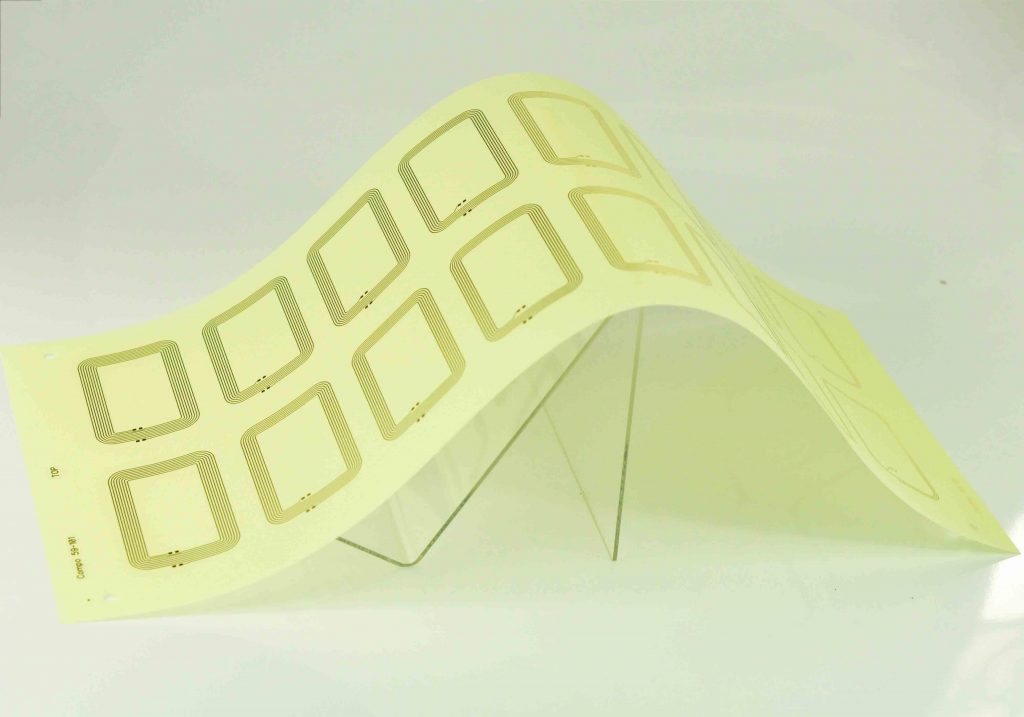
What is the conventional PCB copper thickness?Thick copper plate, FPC

‌Regular PCB copper thickness is 1oz (35μm). When the thickness of the copper foil reaches or exceeds 2oz, such a PCB board is defined as a thick copper board; for flexible circuit boards (FPC), the copper thickness also has different specifications, for example, 0.5oz copper thickness is used for flexible circuit boards is being manufactured. ‌

The influence of copper thickness on PCB

In PCB manufacturing, the choice of copper thickness is determined based on specific application requirements. Common copper thickness classifications include:

1. ‌1oz copper thickness: ‌

This is the most common and standard copper foil thickness and is widely used in everyday electronic devices and general applications. 1oz (ounce) means 1 ounce of copper foil weighs 1 square foot. In the PCB manufacturing process, 1 ounce corresponds to a copper foil thickness of approximately 35 microns, which has good electrical and thermal conductivity.

2. ‌2oz copper thickness: ‌

Copper foil of this thickness is usually used in circuits that require higher current carrying capabilities, such as power amplifiers, high-power LEDs, etc. 2oz copper thickness corresponds to a copper foil thickness of approximately 70 microns, which has better performance in electrical conductivity and heat dissipation than 1oz copper thickness.

3. ‌0.5oz copper thickness: ‌

This thinner copper foil thickness is suitable for some light and small electronic products, such as electronic watches, mobile phones, etc. 0.5oz (18Îźm) copper foil is suitable for equipment that has strict requirements on circuit board size and weight.

How to choose PCB copper thickness?

Choosing PCB copper thickness depends primarily on the board’s purpose, current requirements, signal integrity requirements, cost budget, and manufacturing process capabilities.

1. ‌Circuit board usage and current requirements‌: For circuit boards that need to handle large currents, such as power boards, it is recommended to use thicker copper foil, such as 2oz (about 70μm) or 3oz (about 105μm). For signal transmission, a copper thickness of 1oz (~35μm) is usually sufficient. Ordinary double-sided boards generally use 1oz copper thickness, while multi-layer boards generally use 1/2oz, 1/3oz copper thickness for the inner layer, and 1oz, 1/2oz, 1/3oz copper thickness for the outer layer.

2. Signal integrity requirements: For high-density interconnect (HDI) boards or high-frequency circuits, thinner copper foil may be required to reduce parasitic effects and ensure signal integrity.

3. ‌Cost considerations‌: The thicker the copper foil, the higher the cost is usually.

4. Environmental factors: For PCBs in extreme working environments (such as high temperature, high humidity or high vibration environments), the thickness of the copper foil may need to be adjusted to enhance the stability and durability of the circuit.

In summary, selecting PCB copper thickness is a process that comprehensively considers multiple factors and needs to be determined based on specific application scenarios and design requirements.

What is the difference between different copper thicknesses on PCB?

‌The main differences between different copper thicknesses on PCBs are their conductive properties, load-bearing capacity, anti-interference performance, cost and manufacturing difficulty. ‌

The influence of copper thickness on PCB

‌Outer copper thickness‌ is commonly used for circuit board routing and connections, and its selection depends on the application requirements and design needs of the circuit board. The outer copper thickness range is generally between 1-5oz, and the more common ones are 1oz, 2oz, 3oz and 4oz. The thicker the outer copper layer, the stronger the circuit board’s load-bearing capacity, and the better its anti-interference performance and electrical conductivity. But at the same time, the increase in the thickness of the outer copper layer will also lead to an increase in cost and manufacturing difficulty.

‌Inner layer copper thickness‌ is used for internal connections and signal transmission of the circuit board, and its selection also depends on the application requirements and design needs of the circuit board. The thickness of the inner copper layer generally ranges from 0.5-2oz, with the more common ones being 0.5oz, 1oz, and 2oz. If the circuit board needs to transmit high-speed signals, a larger inner copper thickness should be selected. The increase in the thickness of the inner copper layer will also lead to an increase in cost and manufacturing difficulty.

‌Copper Thickness Standard‌According to international standards, the copper thickness of PCB boards can be divided into standard copper thickness (such as 1oz and 2oz) and non-standard copper thickness (such as 0.5oz, 3oz and 4oz). In practical applications, some special PCB boards may require higher copper thickness, such as high-power LED lights, electronic high-frequency circuits, etc.

To sum up, the choice of different copper thicknesses is to meet specific circuit board design needs, including conductive performance, anti-interference performance and other requirements. At the same time, the choice of copper thickness also needs to consider aspects such as cost and manufacturing difficulty.

Conclusion:

By controlling the thickness of copper on the PCB to meet different usage requirements, applications that require large currents will naturally require PCBs with thicker copper foils. However, PCBs that require thicker copper foils are a great test of the capabilities of PCB manufacturers. BEST Technology has accumulated rich production experience in the PCB manufacturing industry and has many years of manufacturing experience for PCBs with different copper thicknesses. We can meet any PCB copper thickness requirements.

You may also like

Let you know about PCB copper layer thickness
Friday, August 16th, 2024

In the printed circuit board industry, the most common way to express the copper layer thickness on a PCB is in ounces (oz). 1oz means 1oz of copper evenly covers an area of 1 square foot, which is about 1.4mil. It uses the weight of the tissue area to express the average thickness of the copper foil. Expressed in terms of formula, 1oz=28.35g/FT2 (FT2 is square feet, 1 square foot = 0.09290304 square meters).

What is the standard thickness of a copper layer on a PCB?

In the manufacture of printed circuit boards (PCBs), the thickness of the copper layer is an important parameter that directly affects the electrical performance and reliability of the circuit board. Depending on the application requirements, the thickness of the copper layer can vary within a certain range. Generally speaking, the conventional copper layer thickness is between 1-35Îźm, with 35Îźm being the most commonly used thickness. For some applications with high reliability requirements, the copper layer thickness may reach more than 50Îźm.

The selection of the thickness of the copper layer is a decision-making process that takes into account a variety of factors, including the conductivity, heat dissipation, mechanical strength, cost and manufacturing difficulty of the circuit board. A larger copper thickness can reduce resistance and improve the conductivity and heat dissipation of the circuit board, but it will also increase material costs and production difficulties. Therefore, when designing PCB boards, engineers need to select a suitable copper thickness standard range based on specific application scenarios and design requirements to ensure the performance and reliability of the circuit board.

1oz copper thickness in mm = 0.035mm

0.5 oz copper thickness in mm = 0.0175mm

1.5 oz copper thickness in mils = 0.0525mm

2 oz copper thickness in mils =  0.07mm‌

How thick is PCB copper after plating?

PCB printed circuit boards are usually bonded to glass epoxy substrates with a layer of copper foil, usually 18, 35, 55 and 70 microns thick. The most commonly used copper foil is 35 microns thick.

The copper foil used by PCB manufacturers is generally 35~50 microns thick, and some are thinner than this, such as 10 microns, 18 microns, and thicker such as 70 microns. The thickness of the composite copper foil on a 1~3 mm thick substrate is about 35 microns. The thickness of the composite copper foil on a substrate with a thickness of less than 1MM is about 18 microns, and the thickness of the composite copper foil on a substrate with a thickness of more than 5 mm is about 55 microns.

The copper layer thickness of PCB (printed circuit board) can be adjusted according to different needs and designs. Common copper layer thicknesses include 1oz (35μm), 2oz (70μm), 3oz (105μm), and other thicker options. For most applications, a copper layer thickness of 1oz is sufficient and suitable for general signal transmission. ‌For circuit boards that need to carry large currents, such as switching power supplies, a copper layer thickness of 2oz or higher is usually used. ‌In addition, there are some special cases where manufacturers provide extremely heavy copper up to 20 oz/ft2 (26.8 mils or 0.34 mm) to meet special needs. ‌

When choosing the thickness of the copper layer, factors such as the purpose of the circuit board and the magnitude of the signal voltage and current need to be considered. ‌For example, for circuit boards that require excessive current, a copper thickness of 70μm or 105μm may be used. ‌For thin laminates that require ultra-high density patterns, a copper thickness of 12μm may be used. ‌Therefore, the specific thickness of the PCB after copper plating is determined according to design requirements and specific applications.‌

How thick is 2 oz copper for PCB?

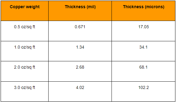
If 1 ounce (28.35 grams) of copper were flattened to evenly cover a surface area of 1 square foot (0.093 square meters), the resulting thickness would be 1.37mils (0.0348mm). A conversion chart for different units of measurement can be found below.

PCB copper layer thickness 

What is the difference between different copper thicknesses in PCB?

‌Copper is an excellent conductive material, and the thickness of the copper layer directly affects the conductive effect of the circuit board. ‌Thicker copper layers can provide lower resistance, reduce signal transmission losses, and are particularly suitable for high-frequency and high-speed digital circuits. ‌

During the operation of electronic equipment, good heat dissipation is a key factor in ensuring the performance and life of components. ‌Thicker copper layers can conduct and dissipate heat more effectively, preventing components from overheating. ‌

In high-power electronic devices, thicker copper layers can carry larger currents, avoiding burnout or performance degradation caused by excessive current.

Below is the conductivity corresponding to different copper thicknesses.

PCB copper layer thickness 

How thick is high current PCB copper?

In PCB design, copper thickness (also called copper thickness) is an important parameter, which directly affects the performance indicators of the circuit board such as current carrying capacity, heat dissipation and reliability. For PCBs that need to withstand high currents, such as high-power LED light strips, power circuit boards, high-power motor control boards or high-power inverter control boards, thicker copper layers are usually used to increase current carrying capacity.

PCB copper layer thickness 

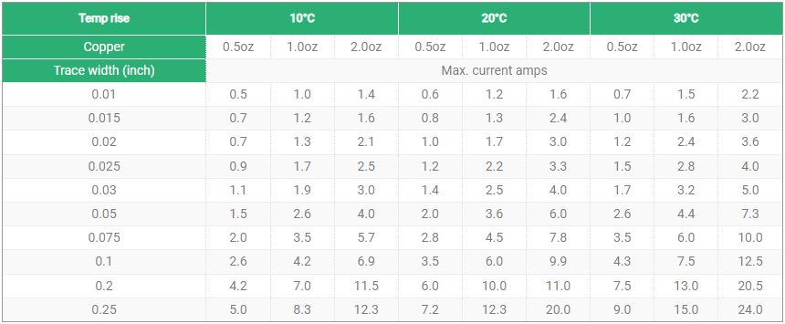
Different uses have different copper foil thicknesses. Common 0.5oz, 1oz, and 2oz are mostly used in consumer and communication products. Thick copper products above 3oz are mostly used for high currents, such as high-voltage products and power boards.

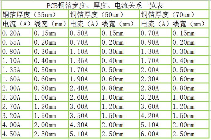
The thickness of copper foil (track width) will affect the current size. Although there is a formula that can directly calculate the maximum current carrying capacity of copper foil, it is not so simple when actually designing the circuit. Therefore, the safety factor should be fully considered during the design.

How thick is the copper in a flex PCB?

The thickness of copper foil in flexible PCB is generally 18Îźm, 35Îźm, 55Îźm and 70Îźm. These thickness specifications are suitable for different types of circuit board requirements, among which 35Îźm is the most commonly used copper foil thickness.

PCB copper layer thickness 

For flexible PCB, the choice of copper foil thickness depends on the specific purpose of the circuit board and the size of the signal voltage and current. For example, for PCBs that require excessive current, some parts will use 70Îźm copper thickness, while for signal transmission, 1oz (35Îźm) thickness is usually sufficient. In addition, for substrates of different thicknesses, the thickness of copper foil is also different. For example, the thickness of the composite copper foil on a 1mm thick substrate is about 18Îźm, and on a substrate thicker than 5mm, the thickness of the composite copper foil is about 55Îźm.

Conclusion:

PCBs for different usage scenarios correspond to different thicknesses of copper, and its thickness directly affects the conductive effect of the circuit board. If the copper layer is too thin, the conductivity may decrease, resulting in signal transmission attenuation or current instability. If the copper layer is too thick, although the conductivity will be very good, it will increase the cost and weight of the circuit board and easily lead to serious glue flow. In PCB manufacturing, it is necessary to select the appropriate copper thickness according to the design requirements and actual applications of the circuit board to achieve the best conductive effect.

BEST Technology is a professional PCB circuit board manufacturer with a large area of site and equipped with useful and experienced production personnel. Corresponding to different thicknesses of copper, we have rich production and processing experience. We can meet the requirements of any circuit board copper layer thickness.‌

You may also like

How to Make SMT? What is SMT Process?
Thursday, August 15th, 2024

What is the SMT?

Surface Mount Technology (SMT) is a production technique used to attach electronic components directly onto the surface of a printed circuit board (PCB). This method enables automated manufacturing to handle most of the assembly process needed to create a functioning board. Components attached in this way are known as surface-mount devices (SMDs). Unlike traditional methods, SMT does not involve inserting components through holes in the board. Instead, components are soldered directly onto the surface using reflow soldering.

Originally known as Planar Mounting, SMT was pioneered by IBM in the 1960s for small-scale computer production, replacing the earlier Through-Hole Technology. However, SMT didn’t gain widespread use until 1986, when surface-mounted components achieved 10% market penetration. By 1990, SMDs had become a dominant feature in most high-tech circuit card assemblies (CCAs).

How to Make SMT? What is SMT Process?

What is the process of SMT manufacturing?

The SMT manufacturing process can be divided into three main stages: solder paste printing, component placement, and reflow soldering. Due to the complexity of the process, each stage is further broken down as follows:

1. Component and PCB Preparation

This initial stage involves selecting surface-mount components (SMCs) and designing the PCB. The board typically features flat copper pads plated with silver, tin-lead, or gold, which are called solder pads. These pads do not have holes and are used to support the pins of components like chips and transistors.

Another crucial element is the stencil, which is aligned with the solder pads to define the placement of solder paste during the next stage. The PCB and all materials involved must be thoroughly inspected to ensure there are no defects before proceeding with production.

2. Solder Paste Printing

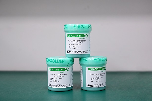
Solder paste printing is a critical phase in SMT production. A stencil and squeegee are used to apply solder paste at an angle of 45° to 60°. The solder paste itself is a combination of powdered metal solder and flux, which temporarily holds components in place and cleans the soldering surfaces of impurities.

The paste is applied to the solder pads, connecting the SMCs to the PCB once melted in the reflow oven. It’s essential that the correct amount of paste is applied to each pad, as improper application can prevent proper connections from forming during reflow.

3. Component Placement

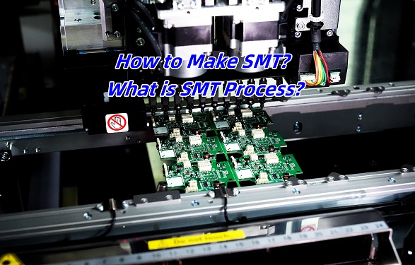
In this stage, pick-and-place machines accurately position components on the PCB. The machines use vacuum or gripper nozzles to remove each component from its packaging and place it onto the board. These machines are fast and precise, capable of placing up to 80,000 components per hour.

Precision is key here, as any misplaced components could lead to costly rework once soldered.

4. Reflow Soldering

After components are placed, the PCB is moved into the reflow oven for soldering. The board passes through several temperature-controlled zones:

  • Preheat Zone

The temperature is gradually increased to between 140℃ and 160℃ at a rate of 1.0℃-2.0℃ per second to ensure the board and components heat evenly.

  • Soak Zone

The PCB is maintained at this temperature for 60 to 90 seconds to stabilize the heat across the entire board.

  • Reflow Zone

The temperature is then raised to 210℃-230℃ to melt the solder paste, bonding the components to the PCB. The molten solder’s surface tension keeps the components in place during this process.

  • Cooling Zone

In the final zone, the solder is rapidly cooled to solidify the connections and prevent any soldering defects.

For double-sided boards, this process may need to be repeated, either using solder paste or adhesive to secure components.

How to Make SMT? What is SMT Process?

5. Cleaning and Inspection

Once the soldering process is complete, the PCB is cleaned and inspected for any defects. This is done using magnifying lenses, Automated Optical Inspection (AOI), flying probe testers, X-ray inspection, and other tools to ensure accuracy. Any flaws are repaired before the finished product is packaged and stored.

What are the basics of SMT?

SMT simplifies assembly by reducing the need for drilled holes and using smaller components. Unlike traditional through-hole components, SMT parts are placed on the surface of the PCB, making the design more compact.

The basic elements of SMT include:

  • PCBs: The base for components, designed with specific pads for each part.
  • Solder Paste: A mixture of metal solder particles and flux, used to create a bond between components and the board.
  • SMT Components: Small electronic parts, such as resistors, capacitors, and ICs, that attach to the PCB.

The transition from through-hole technology to SMT has improved manufacturing speed and performance in electronics.

How do I prepare for SMT?

As the core step of electronic product manufacturing, PCBA’s preparation before assembly directly affects the quality and reliability of the final product. The following is a detailed analysis from multiple dimensions:

1. Component inspection

Before assembly, all electronic components must undergo strict screening and inspection. This includes checking that the component type, package, number of pins, etc. are consistent with the BOM (Bill of Materials), as well as performing the necessary electrical performance tests.

2. Take ESD measures

Static damage to electronic components is invisible, but the consequences are serious. Therefore, when distributing materials and testing IQC, warehouse personnel should wear anti-static gloves, reliably ground the instrument, and lay anti-static rubber MATS on the work surface. During the assembly process, the operator should also wear anti-static clothes, anti-static bracelets and other protective equipment to ensure that the workbench and equipment are well grounded.

3. Cleanliness requirements

The work workshop and workbench must be kept clean to prevent contaminants such as dust and impurities from entering the circuit board, affecting the accuracy and quality of the patch. Clean the work surface and workshop floor regularly. Smoking, eating and drinking are strictly prohibited in the work area.

How to Make SMT? What is SMT Process?

4. Temperature and humidity control

Appropriate temperature and humidity should be maintained in the workshop to reduce static electricity generation and the impact on electronic components. It is usually recommended that the temperature be controlled at 23Âą3oC and the humidity be controlled at 45% to 70%RH. This environment helps to ensure the quality of welding and the stability of electronic components.

5. PCB appearance check

Before assembly, the PCB board should be visually inspected to confirm whether it is complete, whether the surface coated solder resistance layer is intact, and whether there are obvious short circuits and defects. Use a multimeter to check whether there is a short circuit between the power supply and the ground terminal on the printed board, and ensure that the printed board is fine.

6. Check the software and hardware

When the PCBA needs to be upgraded, the motherboards produced in different time periods should not be mixed together to avoid mixing problems. Before assembly, check whether the final use of the software is in accordance with customer requirements to ensure that the software and hardware are compatible and correct.

7. Welding process selection

According to the layout of the circuit board and the characteristics of the components, select the appropriate welding process (such as wave soldering, reflow welding, hot blast furnace welding, etc.). Each welding method has specific requirements for the placement, orientation and spacing of components that need to be planned in advance.

8. Manually prepare the post-welding plug-in components

For some components that cannot be automatically welded (such as large connectors, heat sinks, etc.), manual plug-in assembly is required. This requires the operator to have a wealth of experience and skilled skills to ensure the accuracy and robustness of the plug-in.

9. Perform ESD operations

During operation, use an ESD workbench and an ESD container to hold components and semi-finished products. All welding equipment should be grounded, the electric soldering iron must be anti-static type, and tested before use.

10 Cleaning and protective treatment

After the assembly is complete, the product needs to be cleaned to remove the residue and contaminants generated during the welding process. At the same time, appropriate protective treatment of the product, such as spraying three anti-paint, etc., to improve the product’s moisture, dust and corrosion resistance.

Which solder paste is used in SMT?

The type of solder paste used in SMT assembly process depends on several factors, such as the materials of the components and the PCB, as well as the operating conditions of the finished product. Generally, there are mainly include high temperature solder paste, ‌ medium temperature solder paste and low temperature solder paste. ‌

  • High temperature solder pastes are commonly used in applications where higher temperatures are required for welding. ‌ has a higher melting point and ‌ is suitable for welding electronic components with specific temperature requirements. ‌
  • Medium temperature solder paste and low temperature solder paste are suitable for medium and low temperature welding respectively, ‌ select the appropriate solder paste type according to the specific welding needs. ‌
How to Make SMT? What is SMT Process?

In addition, ‌ solder paste can also be classified according to the flux activity level, ‌ including “R” (‌ inactive) ‌, ‌ “RMA” class (‌ moderate activity) ‌, ‌ “RA” class (‌ completely reactive) ‌ and “SRA” class ‌ (‌ super activity). ‌ Different types of activity levels are suitable for different application scenarios, ‌ for example, ‌ “R” grade is usually used for welding aerospace, ‌ avionics products, ‌ and “RA” grade is suitable for consumer electronics products. ‌ This classification allows users to choose the right solder paste according to the specific application needs and cleaning process requirements. ‌

What temperature should a soldering iron be for SMT?

The right temperature for soldering in SMT can vary depending on the solder paste and components you’re using. Typically, the soldering iron should be set between 250°C and 300°C. Using a lower temperature might not properly melt the solder, while a higher temperature could damage components or the PCB.

Of course, different types of PCB requires different temperature. For example, ceramic PCBs has fragile surface, so a lower temperature is good.

What are the disadvantages of SMT?

  • Small volume (due to the limitation of components)
  • Fragility
  • High soldering requirements
  • Easily damaged or dropped
  • Challenging to inspect
  • Complex process and inspection
  • High equipment investment

How to solder SMT at home?

Soldering SMT components at home can be tricky, but with the right tools and techniques, it’s doable. Here’s a quick guide:

  1. Tools: You’ll need a fine-tip soldering iron, tweezers, solder paste, and flux. You may also want a magnifying glass or microscope for better visibility.
  2. Apply Solder Paste: Use a small amount of solder paste on the pads of the PCB where you want to place your components.
  3. Place Components: With tweezers, carefully place the components onto the solder paste. Make sure they are properly aligned with the pads.
  4. Reflow the Solder: If you have a reflow oven, you can use it to heat the board. Alternatively, a hot air rework station can also work.
  5. Inspect: Once the solder has cooled, check the connections. If necessary, reheat or add more solder to fix any weak joints.

Best Technology is a one-stop PCB & PCB assembly manufacturer founded in 2006, with 5 assembly lines. If you have needs for PCB and PCBA fabrication, we can be your reliable supplier from prototypes to bulk production. In addition, we have SMT factory in Vietnam, if you don’t want to make smt in Shenzhen, then we can support you in Vietnam. Welcome to contact us if you have such PCB and PCBA projects.

You may also like

Rigid flex pcb Design & Prototype Right the First Time
Monday, August 12th, 2024

rigid-flex printed circuit board ,Rigid flex pcb manufacturer. More than 5 years design team of 10 people. Quick proofing within 1 week. A 3,000-square-meter factory for small batch to mass production and assembly.

What is a rigid flex pcb?

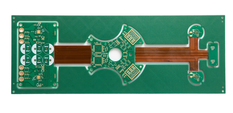
Rigid flex pcb,rigid-flex printed circuit board,Rigid flex circuit are a hybrid construction flex circuit consisting of rigid and flexible substrates which are laminated together into a single structure. Each layer of rigid-flex circuit are electrically interconnected by plated through holes (PTH), which is different from a flexible circuit with FR4/PI stiffener on top or bottom of flex circuit only by the means of presensive or thermal senstive adhesive only, no PTH.

What is a rigid flex pcb?

Rigid-flex PCBs can be divided into single-sided boards, double-sided boards and multi-layer boards according to the number of conductive circuit layers. Multi-layer boards usually contain multiple rigid layers and flexible layers, and the circuits are connected and interconnected through interlayer connections.

Is Rigid flex PCB reliable?

  1. Design and manufacturing efficiency: Designers of rigid-flex boards can use a single component to replace a composite printed circuit board connected by multiple connectors, multiple cables and ribbon cables, which not only has stronger performance and higher stability, but also limits the scope of the design to one component, optimizing the available space by bending and folding the lines like a stacked paper swan.
  2. Space and weight optimization: In PCB prototyping for consumer electronics, the use of rigid-flex boards not only maximizes space use and minimizes weight, but also greatly improves reliability, eliminating many needs for solder joints and fragile and fragile wiring that are prone to connection problems. The design of this circuit board allows the size and weight of equipment and systems to be reduced while maintaining functionality.
  3. High stress environment adaptability: Rigid-flex boards also have high impact resistance and can survive in high stress environments, which makes it widely used in military, aviation and medical equipment.
  4. Excellent electrical performance: Rigid-flex boards provide excellent electrical performance, and good thermal conductivity makes components easy to cool. The lower dielectric constant of the flexible part allows for fast transmission of electrical signals, and the PI substrate has a higher glass transition temperature or melting point, which allows the components to operate well at higher temperatures.
  5. Assembly reliability: Rigid-flex boards reduce the hardware required for traditional rigid boards and flexible boards to be connected, such as traditional jumper sockets, etc., and can provide higher assembly reliability.

What is the difference between rigid flex and semi flex?

  1. Definition and structure
    Rigid-flexible board: It is a combination of soft board and hard board, that is, a thin layer of flexible bottom layer and rigid bottom layer are combined and laminated into a single component to form a circuit board1. It changes the traditional flat design concept and expands it to a three-dimensional space concept. It has both rigid layer and flexible layer and is a multi-layer printed circuit board.
    Semi-flexible board: It is a PCB used in the field of static bending obtained by combining controlled deep milling or rigid-flexible board processing technology (such as milling cover or opening window, etc.) in the standard hard board processing process2. It often uses FR4 material, first processes the PCB according to the normal process, and then mills the middle part that needs to be bent to make it flexible.
  2. Flexibility and application
    Rigid-flexible board: It has higher flexibility and can be bent, folded or rounded, and then integrated into various products, such as aerospace equipment, military aircraft, high-end medical equipment, digital cameras, portable cameras and high-quality MP3 players. ‌
    Semi-flexible board: Although it can be bent or curved, its flexibility is not as good as that of rigid-flexible board. It is mainly used in situations where static bending is required, such as endoscopes in medical equipment, injection needle tip protection circuit boards, and medical equipment temperature control circuit boards. ‌
  3. Processing and cost
    Rigid-flexible board: Due to the mixed use of multiple materials and multiple production steps, its processing time is longer and the production cost is higher. ‌
    Semi-flexible board: Although its processing process is also more complicated, its processing cost is lower than that of rigid-flexible board, and it is more suitable in some applications. ‌
  4. Features and advantages
    Rigid-flexible board: It has stronger performance and higher stability, can reduce space and weight, and improve the reliability of connection. ‌
  5. Semi-flexible board: It has the advantages of low cost, good dimensional stability, bendable three-dimensional installation to reduce space, and reduce the number of interfaces during assembly to improve reliability.‌

how do they add rigid layers to flex pcb?

  1. Design layout: Before starting the manufacturing process, the PCB design layout is first carried out to determine the location and connection method of the components. ‌
  2. Substrate preparation: Clean the laminate containing the copper layer to prepare for the subsequent manufacturing process. ‌
  3. Pattern generation: The generation of circuit patterns is completed by screen printing or photo imaging. ‌
  4. Etching process: The laminate with the circuit pattern is soaked in an etching tank or sprayed with an etchant solution for etching. ‌
  5. Mechanical drilling: Circuit holes, pads and via patterns are drilled using a precision drilling system or technology, such as laser drilling technology. ‌
  6. Copper plating process: Deposit the required copper in the plated vias to establish electrical interconnections between layers. ‌
  7. Covering layer application and lamination: Apply the covering layer material (such as polyimide film) and adhesive, and laminate under specific temperature, pressure and vacuum limits to ensure proper adhesion of the covering layer. ‌
  8. Apply stiffeners: Apply local additional stiffeners before additional lamination processes as required by the board design. ‌
  9. Flexible board cutting: Cut flexible boards from production panels using hydraulic punching methods or specialized punching knives. ‌
  10. Electrical testing and verification: Conduct electrical testing in accordance with IPC-ET-652 guidelines to confirm that the insulation, connection, quality, and performance of the circuit board meet the requirements of the design specifications.

What are the disadvantages of rigid flex PCB?

  1. Material damage or breakage: The flexible materials used in rigid-flex boards are susceptible to flexure and bending. Long-term use or improper handling may cause damage or breakage of the flexible part, resulting in an open circuit.
  2. Poor welding: The manufacture of rigid-flex boards requires welding processes. If the welding is poor or the solder joints are of poor quality, it may cause loose connections or solder joints to fall off, resulting in an open circuit.
  3. Excessive bending or stretching: Excessive bending or stretching during use may cause the connection wires or wires of the flexible part to be stretched excessively and break, causing an open circuit.
  4. Design defects: If the design of the rigid-flex board is unreasonable or defective, such as insufficient design of the overbending area or too small bending radius, the material of the flexible part may be damaged by excessive stress, resulting in an open circuit.
  5. Environmental factors: Under different environmental conditions, it may be affected by factors such as temperature, humidity, and chemicals. Long-term use in harsh environments may cause material aging or corrosion, resulting in an open circuit. ‌
  6. Damage during assembly: During the assembly process, improper operation or external force may cause damage to the connecting wires or wires of the flexible part, resulting in an open circuit.

Application fields of rigid flex PCB

  1. Automotive electronics: Rigid-flex boards are widely used in automotive electronic systems such as dashboards, navigation systems, and in-car entertainment systems in the automotive industry. Their flexibility and high reliability enable them to adapt to the complex spatial layout and vibration environment inside the car.
  2. Medical equipment: In the field of medical equipment, rigid-flex boards also have important applications, such as medical monitoring equipment, medical imaging equipment, etc. Its flexible part can adapt to different equipment shapes and size requirements, while having stable circuit connection performance.
  3. Aerospace field: Rigid-flex boards are usually used in aircraft dashboards, navigation systems, communication equipment, etc. in the aerospace field. Due to their light, thin and flexible characteristics, rigid-flex boards have become an ideal choice for aerospace equipment.
  4. Smart wearable devices: With the rapid development of smart wearable devices, rigid-flex boards are widely used in products such as smart watches and health monitoring equipment. They can be combined with curved display screens, sensors and other components to achieve a more humanized design.
  5. Industrial control field: In the field of industrial automation control, rigid-flex boards are often used in PLC controllers, robot control systems, sensor interfaces, etc. Its flexibility and reliability ensure the stable operation of the equipment in harsh environments.
Application fields of rigid flex PCB

Rigid flex pcb manufacturer

rigid flex pcb.rigid-flex printed circuit board,Rigid flex circuit are a hybrid construction flex circuit consisting of rigid and flexible substrates which are laminated together into a single structure. Each layer of rigid-flex circuit are electrically interconnected by plated through holes (PTH), which is different from a flexible circuit with FR4/PI stiffener on top or bottom of flex circuit only by the means of presensive or thermal senstive adhesive only, no PTH.

Rigid flex pcb manufacturer

Multilayer circuitry-from 3 to 14+ layers
Min LW/LS: 4mil/4mil
Adhesive-based and adhesiveless constructions, including thermoplastic and thermoset stiffener attachment.
Polyimide substrates: 1/2mil – 4mil
Copper: 1/3OZ – 2OZ, RA or ED type
Stiffeners include Polyimide (0.075-0.20mm), FR4 (0.15-2.0mm), and punched or formed metal parts (0.075-1.0mm)
Low-cost, conventional fabrication and lamination completed with PTH based plating
Screened inks, photo-imageable soldermasks, or laminated coverlay dielectrics
Surface finishes: ENIG, electroplated nickel/gold, immersion silver, tin,
EMI Shielding

how to design flex rigid pcb?

Rigid-Flex Circuit Design Guidelines

To form a rigid-flex, follow these considerations to ensure the best results.

Considerations When Designing Rigid-Flex Circuits

To produce a rigid-flex PCB with unmatched quality and functionality, you must follow the correct manufacturing specifications. This is the set guidelines and standards that manufacturers must consider when designing and manufacturing flexible circuit boards.

Determine Manufacturing Process and Materials Beforehand

Depending on the flexibility you require, you need to decide beforehand what materials to use and the methods to use. Example; When the board you are designing only needs to be folded during manufacturing and thereafter be in a fixed position without bending, you can decide the following

  1. Copper type and grade
  2. Manufacturing method
  3. Number of layers to be used.

On the other hand, if the board is for an application with frequent movement, vibration, and impact, you must be clear in choosing the following:

  1. Copper Coils
  2. Adhesives and
  3. Number of Layers

Place Copper Traces at Right Angles to Rigid-Flex

Copperworks is a great fit when placed on the right edge of the board. Avoid bending copper traces at corners as it will pull stress and may not create the best bend. For PCB flex that requires bending, use sharp radius bends to avoid smudging copper traces.

Provide adequate pad support for exposed copper

Repetitive stress from frequent bending can cause copper on the circuit to break away from the polyimide substrate. Support exposed copper with pads to prevent separation.

Use hatched polygons

Hatched polygons instead of solidified copper help maintain the flexibility of flexible PCBs.
Leave at least 1/2mm gap between copper ring and adjacent vias

1/2mm helps avoid fatigue caused by frequent bending. Placing vias in fixed areas of the board helps avoid frequent movement and bending, resulting in the best rigid-flex.

You may also like

What is Tda7294 amplifier board &tda7294 datasheet
Wednesday, August 7th, 2024

TDA7294 is a class AB monolithic audio amplifier integrated circuit launched by SGS-THOMSON Microelectronics in the 1990s. It swept away the raw, cold and hard sound of previous linear integrated amplifiers and thick film integrated amplifiers, and is widely used in HiFi fields, such as home theaters, active speakers, high-performance TVs and other fields.

The chip adopts a 15-pin dual-row asymmetric plug-in package, the differential input stage is composed of bipolar transistors, and the driver stage and power output stage use DMOS field-effect transistor semiconductor technology. This hybrid semiconductor manufacturing process allows TDA7294 to take into account the advantages of bipolar signal processing circuits and MOS power tubes, and the playback sound is very friendly (it is praised by audiophiles as a “tube-flavored amplifier”); the built-in silent standby function, short-circuit current and overheating protection functions make its performance more perfect. It can be used in HiFi home audio, active audio, high-performance TVs and other fields.

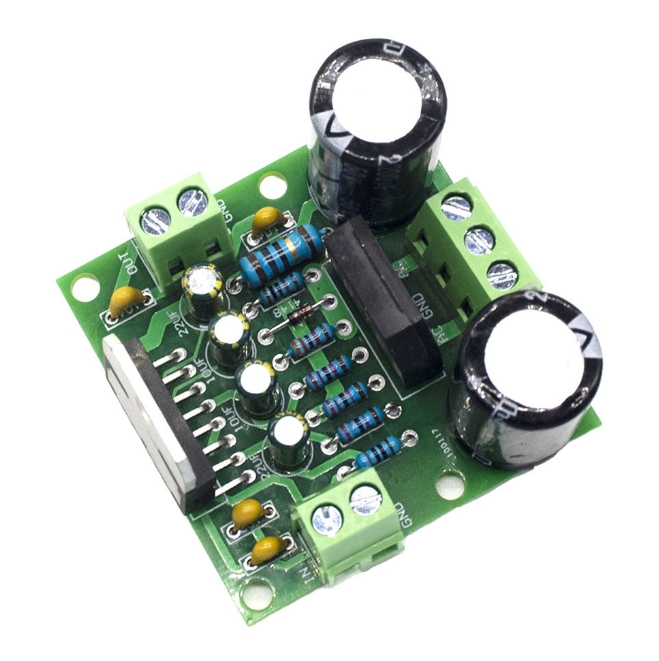
Tda7294 amplifier board

tda7294 amplifier board

tda7294 amplifier board PCBA

  1. This circuit is an official standard circuit, stable and reliable.
  2. The filter uses a large electrolytic capacitor with a withstand voltage of 50V and a capacity of 2200uf.
  3. Power supply voltage: dual 12-36V ring transformer, dual 32V ring transformer is recommended
  4. Output power: 85W*1 undistorted rated power, peak power 100W
  5. Can easily drive speakers above 100W, speaker impedance: 4-8 ohms
  6. PCB size: 50*50mm
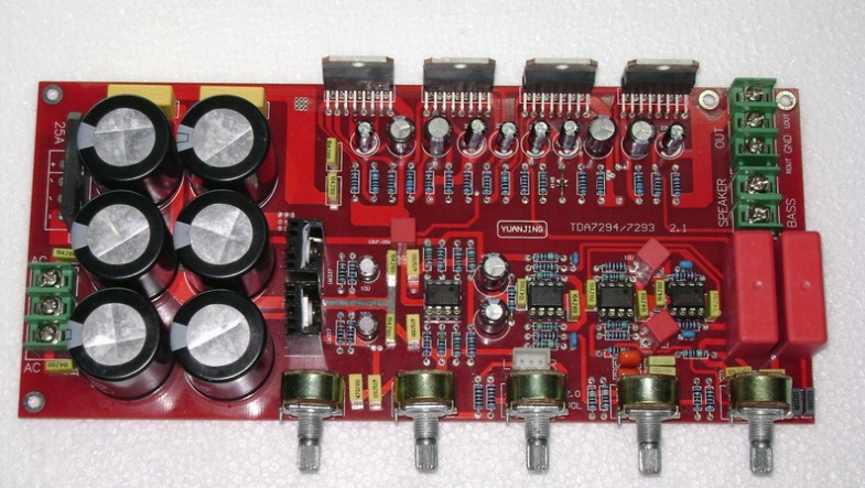
tda7294 amplifier board

Basic parameters:
Power supply: dual 18-28V AC
Power: 2X80W+160W subwoofer
Circuit board size: 218x98MM
Potentiometer function: low frequency frequency adjustment, subwoofer volume. Left and right channel volume, treble, bass.

Adopting the new laser dark word TDA7294
The power filter uses 6 63V3300UF capacitors, and the rectifier uses a 25A imported rectifier flat bridge.
PCB uses 1.6mm thick double-sided board, 2.0 ounces copper thickness, and full tin spraying process to ensure good passing performance of large and small currents.
Fever component assembly, the subwoofer part consists of two new TDA7294 BTL output,
The low-pass filter is designed according to the frequency adjustable design of home theater style (50-150HZ), with strong power!
The left and right channels are served by two TDA7294 respectively, and the input coupling capacitor uses the German imported WIMA 2.2UF coupling capacitor, which makes the sound sweeter!
The signal-to-noise ratio of the board is also very high, and even if you put your ear close to the speaker, you can’t hear the AC noise! ​​It is the best choice for upgrading 2.1 amplifiers!

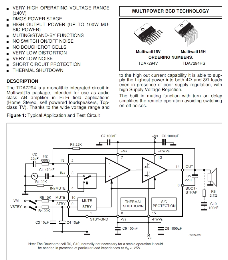
TDA7294 datasheet

TDA7294 datasheet
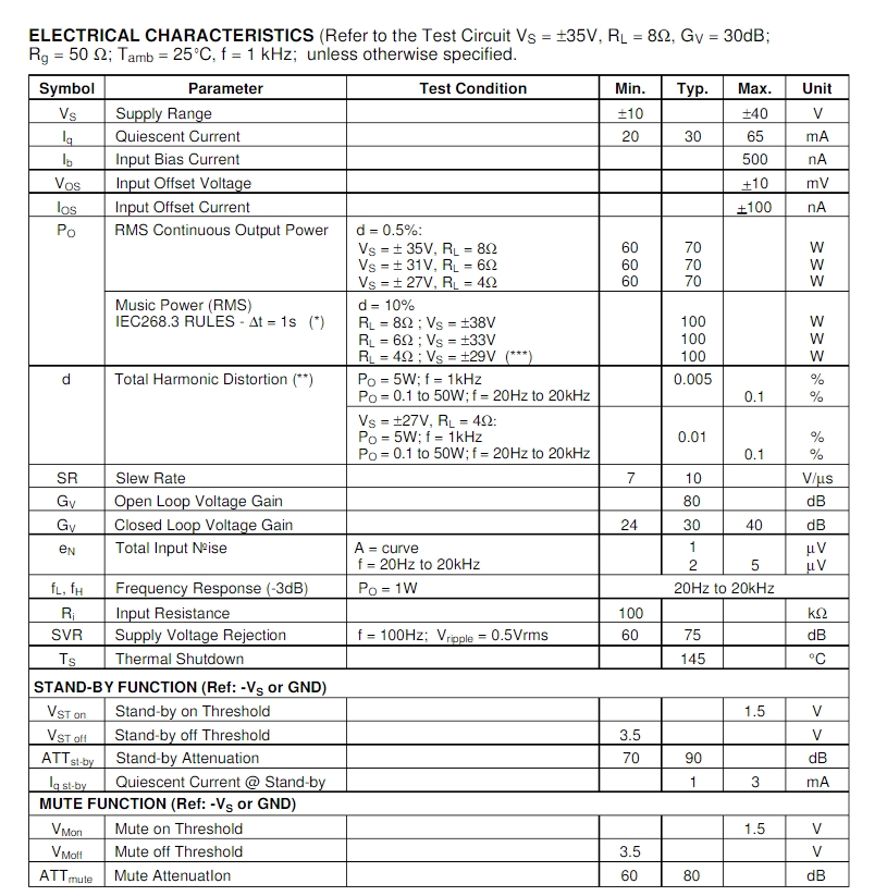
TDA7294 datasheet

TDA7294 Main Features

Wide supply voltage range: Âą10V ~Âą40V
High output power: 70W (up to 100W)
Standby and mute functions
Noiseless ON/OFF switch
Low noise and low distortion
Short circuit protection and overheat protection

TDA7294

Pin function
Pin 1 is the standby terminal;
Pin 2 is the inverting input terminal;
Pin 3 is the positive input terminal;
Pin 4 is grounded;
Pins 5, 11, and 12 are empty pins;
Pin 6 is the bootstrap terminal;
Pin 7 is +Vs (signal processing part);
Pin 8 is -Vs (signal processing part);
Pin 9 is the standby pin;
Pin 10 is the mute pin;
Pin 13 is +Vs (final stage);
Pin 14 is the output terminal;
Pin 15 is -Vs (final stage)

DIY Production

1) The first step is to get the PCB. Here you can make the PCB yourself by DIY ironing method. Since the PCB is easy to make, the PCB design is kept single layer only, or you can get ready-made quality PCB from best.or custom tda7294 amplifier board.
2) After the PCB is completed, carefully mount all small components like jumpers, resistors, diodes, etc. to the PCB and trim their terminals, then solder them to the PCB first, because there are many components on this board, so it is better to solder them one by one
3) After installing the small components, install the large components like capacitors, fuse holders, rectifiers to the PCB and solder them. (Don’t install the power filter capacitor, 22000uF capacitor for now. Completed in the following steps)
4) After that, it’s time to mount all 7 ICs to the PCB and solder them.
5) Now properly mount the heat sink on the IC using insulating MICA and insulating plastic shoulder washers. Remember to use good quality thermal paste between the heat sink and IC.
6) After mounting the IC on the heat sink. Check the continuity between the heat sink and the IC back plate using a multimeter. There should not be any continuity between them. Please note the heat sink isolation
7) Now mount the cooling fan to the PCB using cable ties or any other suitable method.
The board assembly is now complete. Clean the track side of the board using IPA (Isopropyl Alcohol) or cleaning flux and then power the board using a 20-0-20 VAC transformer or a 24-0-24 VAC transformer.

Which one has better sound quality, TDA7294 or LM3886? Voltage AC 28v

LM3886 has better bass because its maximum current can reach 10A, which means it can drive a 2-ohm box without any problems. From the parameters alone, LM3886 is worse than 7294. And it is true in practice, especially for bass. If the transformer is OK, it feels very powerful. 7294 is not as good as 3886 in bass. The current is large when it comes to bass. 7294 itself has overcurrent protection. When the current reaches a certain level, it starts to limit the output current. However, 7294 is better in treble.

You may also like

PCB vs CCA: What is a Circuit Card Assembly?
Monday, July 22nd, 2024

Hey there! If you’re curious about circuit card assembly (CCAs) and what makes them tick, you’ve come to the right place. CCAs are the unsung heroes behind many of the electronic devices we use every day. Let’s dive into what they are, their essential parts, how they’re made, and why they’re so important.

What is a circuit card assembly?

Circuit card assembly or CCA is the process of producing printed circuit boards. In essence, it is the same as PCBA (PCB assembly), just in different name. CCA is a manufacturing technology that converts raw materials into printed circuit boards. It is used in many industries, including the military and aerospace sectors. This type of manufacturing requires skilled professionals to lay out the design and then assemble it. If you are planning to buy a batch of circuit card components, here are some things you should know about CCA.

PCB vs CCA: What is a Circuit Card Assembly?

A circuit card is a thin, flat dielectric material on which conductive paths or traces are etched. These paths connect various electronic components. They are also used to connect components to sockets on printed circuit boards. Circuit card assy is the process of manufacturing circuit card components. The process involves adding electronic components to the substrate.

Key components of a circuit card assembly (CCA)

Circuit card assembly have several key components to make the circuit function properly. These can be divided into three basic components.

  • Printed Circuit Board (PCB)
  • Electronic component
  • Solder paste
  • Printed Circuit Board (PCB)

This is the backbone of the CCA. The printed circuit board provides the structural foundation on which all other components are mounted. A PCB is typically made of a flat, insulating material such as FR4 fiberglass, which is layered with conductive tracks made of copper. These tracks form the circuit pathways that connect various electronic components. The PCB board can be single-sided, with components and conductive tracks on one side only, or double-sided, with tracks and components on both sides. For more complex applications, multi-layer PCBs are used, which consist of multiple layers of insulating material and conductive pathways stacked together. These printed circuit boards are essential in ensuring that electrical signals are routed efficiently and reliably across the assembly.

PCB vs CCA: What is a Circuit Card Assembly?

  • Electronic Components

These include resistors, capacitors, integrated circuits, transistors, and more passive and positive components. Each part plays a specific role in the circuit, like pieces of a puzzle fitting together to make a complete picture. Resistors control the flow of electrical current, capacitors store and release energy, integrated circuits (ICs) perform various functions like processing and memory storage, and transistors act as switches or amplifiers. These components are carefully placed on the PCB in positions that allow them to connect and interact as designed.

PCB vs CCA: What is a Circuit Card Assembly?

  • Solder paste

Solder paste is like the glue that holds everything together, but it’s electrically conductive. It’s used to attach the electronic components to the PCB, so that they can stay put and work properly. Soldering creates a strong, conductive bond between the component leads and the PCB’s copper tracks. There are different types of soldering, such as lead-based and lead-free solders, each with its specific properties and applications. The soldering process can be done manually or using automated printing machines, depending on the complexity and volume of the assembly. Please noticed that solder paste should used in a very short time, otherwise, it will become dry solder paste.

PCB vs CCA: What is a Circuit Card Assembly?

What is the Difference Between a PCB and a CCA?

You might wonder, what’s the difference between a PCB and a CCA? Well, here’s a quick rundown:

AspectPCB (Printed Circuit Board)CCA (Circuit Card Assembly)
DefinitionA blank board with conductive pathwaysA PCB populated with electronic components
ComponentsNo electronic componentsIncludes electronic components like resistors, capacitors, ICs
FunctionalityServes as the foundation for electronic circuitsA functional electronic circuit ready for use in devices
Manufacturing StepsInvolves design, etching, and printing of conductive pathsInvolves PCB manufacturing plus component placement and soldering
Usage StageIntermediate stage in manufacturingFinal stage, ready for integration into electronic devices
ComplexityLess complex, involves fewer manufacturing stepsMore complex, involves multiple stages of assembly and testing

What is the circuit card assembly manufacturing process?

Making a CCA is a multi-step process:

Design

First, the PCB layout is designed using computer software. It includes numerous steps, like schematic drawing, layout design, SI, PI analysis, DFM. This can ensure the PCB board can fit all the necessary components and function correctly.

Fabrication

The PCB is then fabricated, which involves creating the physical board with layers of insulating and conductive materials. This is where the board gets its pathways. In this step, proceed strict quality control process to make sure the bare boards are qualified.

Component Placement

Next, printing solder paste and preparing components, then place them onto the PCB board according to the BOM file (bill of material). After setting up the pick and place machine, automated machines can precisely position each component based on the design.

Soldering

The components are soldered to the PCB. This can be done using methods like wave soldering or reflow soldering to ensure everything is securely attached and electrically connected. You must know, different products require different parameters, please make sure all the parameters like temperatures, time are suitable.

Inspection and Testing

The assembled CCA goes through rigorous inspection and testing to ensure it works as intended. This includes visual inspections, automated optical inspections (AOI), in-circuit testing (ICT), aging testing and functional testing.

Final Assembly

If the CCA passes all tests, it moves on to final assembly, where it’s integrated into the larger electronic system or device. That is we say the box building assembly.

What are the types of circuit card assembly?

CCAs can be divided into various types according to the different manufacturing technology.

Through-Hole Technology (THT) Assembly

Here, components have leads or pins inserted into holes drilled through the PCB and soldered on the other side. This method provides strong mechanical bonds, making it great for components that experience mechanical stress. It’s often used in aerospace, military, and industrial equipment.

Surface Mount Technology (SMT) Assembly

In SMT, components are mounted directly onto the PCB surface using solder paste. No drilling required, which allows for higher component density and smaller PCBs. This method is commonly used in consumer electronics, telecommunications, and automotive industries.
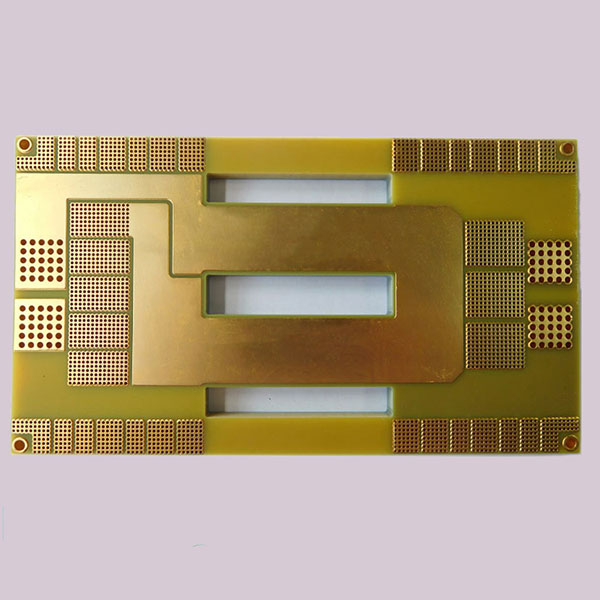
Box Building Assembly

Box building assembly involves the complete assembly of electronic systems, including CCAs, into enclosures or boxes. This process includes not only the assembly of the PCB but also the integration of cables, connectors, and other components into a final product. Box building is ideal for producing complete electronic devices ready for end-use.

Advanced materials for CCAs

Advanced materials help CCAs perform better and last longer:

  • High-Temperature Laminates (e.g., FR-4, Polyimide)

High temperature laminate like FR4 or polyimide. These materials can handle extreme conditions without breaking down. FR-4 is popular for its excellent thermal and mechanical properties, while polyimide is great for high-temperature stability.

  • Flexible Substrates (e.g., Kapton, PET)

Kapton and PET are the most common flexible substrate. These materials allow CCAs to bend and flex. Kapton, a type of polyimide, is known for its high thermal resistance and flexibility, making it perfect for wearable electronics and medical devices. PET (polyethylene terephthalate) is another flexible material with good electrical insulation properties.

  • Advanced Solder Compounds

SAC305 (a lead-free alloy of tin, silver, and copper) is favored for its mechanical and thermal properties. Whatever you want to mount a ceramic PCB or the flexible PCB, it is the best choice. Sn63Pb37, a traditional tin-lead solder, is still used for its ease of use and excellent performance.

Reliable circuit card assembly manufacturers

Choosing the right manufacturer for your CCAs is key to getting quality products. PCBonline and Best Technology are go-to-choice reliable circuit card assembly manufacturers. Both of them has advanced pick and place machine, full-auto SPI, AOI equipment, ensuring a good quality.

As a leading manufacturer in the circuit card assembly, Best Technology prides full turn-key service, ranging from the PCB design, PCB fabricating, electronic component sourcing, circuit card assembly and box build assembly. We handle complex and high-volume orders efficiently, ensuring timely and fast delivery without sacrificing quality. In 2023 alone, we completed over 5000 high-complexity projects with a client satisfaction rate of over 98%.

It is crucial for anyone to fullly understand the circuit card assembly in the electronics industry. From their basic components and manufacturing process to the advanced materials used, CCAs are the backbone of modern electronic devices.

You may also like

How to Make a BOM?
Thursday, July 11th, 2024

If you are familiar with SMT or PCB assembly process, you may know BOM file. It is an important element in the SMT process. Creating BOM is a crucial step in the manufacturing process, especially for PCBs. A BOM serves as a comprehensive list of all the parts, components, and materials needed to build your product. It ensures that everyone involved in the production process is on the same page, reducing the risk of errors and delays. Today, Best Technology would like to introduce BOM and giving you a guide to create a BOM file step by step.
How to Make a BOM?

What is a Bill of Materials (BOM)?

A Bill of Materials (BOM) is a detailed list of all the parts, components, and materials needed to manufacture a product. In PCB manufacturing, a BOM outlines every item required to assemble a PCB, including quantities, part numbers, and descriptions. It serves as a guide to ensure that the manufacturing process runs smoothly and that no crucial components are missing.

Types of Bill of Materials

There are several types of BOMs used in different stages of production. Each type serves a specific purpose and provides unique details to streamline processes and ensure accuracy. Here are the primary types of BOMs:

  • Engineering BOM

This type of BOM is creating during the design phase. It lists all the parts and components designed by the engineering team, including specifications and relationships as intended in the final product. And of course, it mainly used by design engineers to communicate the product structure and details to manufacturing teams.

  • Manufacturing BOM (Formal)

It is a formal BOM files that used in the assembly phase. Different with engineering BOM, it includes additional details necessary for manufacturing, such as packaging, handling instructions and assembly details. And some special instructions.

  • Sales BOM

Sales BOM is used by sales teams and includes information relevant to the sales process, such as pricing and availability. It helps in providing accurate quotes, managing customer expectations, and handling sales orders efficiently.

What Should Include in an Effective Bill of Materials?

An effective BOM should be detailed, accurate, and easy to understand. It should include all the details of components and indicated revisions. As a 18 years expertise in PCBA production, we summarized the key elements that should be included in the BOM.

  • Component details

It should include all the components and their detailed information, such as names, part numbers (PN), and descriptions for each part.

  • Quantity (QTY)

The exact quantity of each component required for the product. Accurate quantities can prevent shortages and overstocking.

  • Foot print

It is the package of each component, helping to ensure the correction of part.

  • Reference Designators

Unique identifiers that match each component to its specific location on the product layout. These are essential for assembly and troubleshooting.

  • Manufacturer Information

Manufacturer information, including the manufacturer name of components and manufacturer part number. It helps to ensure correct parts are sourced. And convenient for alternative part sourcing if it is shortage.

  • Supplier information (Optional)

It means the name of the supplier or distributor. The part number used by the supplier, which may differ from the manufacturer’s part number.

  • Assembly instructions

Any special notes for assembly such as DNF remark, and version control to track revisions should also be included. Additionally, cost information helps in budgeting, and lifecycle status information helps plan for component availability and avoid discontinued parts.

How to Make a PCB Bill of Materials (BOM)?

Creating a PCB BOM is a systematic process that involves compiling all the necessary information about each component required for the assembly of the PCB. Here’s a detailed guide on how to create a PCB BOM:

  • Open a Blank Spreadsheet

Use software like Microsoft Excel or Google Sheets to start with a blank spreadsheet. They are common to use, offering flexibility and ease of use for creating and managing BOMs.

  • Define Columns

Set up your spreadsheet with appropriate column headers. Common headers include:

  • Part Number
  • Component Name
  • Quantity
  • Reference Designator
  • Manufacturer
  • Manufacturer Part Number
  • Supplier
  • Supplier Part Number
  • Description
  • Package Type
  • Cost
  • Notes
  • Input Data

Enter the required details for each component under the appropriate headers. Please be make sure that all information is accurate and complete. This may involve referencing design files, datasheets, and supplier catalogs. If it is incorrect, then it needs a lot of time to find out and revise the errors, resulting in schedule delay.

  • Use Formulas

Utilize Excel formulas to automate calculations, such as summing total quantities or calculating costs. This helps in reducing manual errors and saves time.

  • Format for Clarity

Use cell formatting options to highlight important information and ensure the spreadsheet is easy to read. For example, you can use bold text for column headers, color coding for different component types, and borders to separate sections.

  • Include Version Control

Add a version control section to your BOM to track revisions and updates. This can be a simple row at the top or bottom of the spreadsheet, indicating the version number, date of revision, and a brief description of changes.

How to Make a BOM?
(BOM file reference)
  • Save and Update

Save your BOM and update it regularly to reflect any changes in the design or component availability. Regular updates ensure that the BOM remains accurate and up-to-date, preventing issues during production.

  • Review and Verify

Have multiple team members review the BOM for accuracy. Cross-check all component details, quantities, and part numbers against the design files. Verification helps catch errors early and ensures the BOM is reliable.

  • Communicate with Suppliers:

Maintain open communication with suppliers to confirm component details and availability. This ensures that you can source the correct parts and avoid delays in the production process.

How Can I Optimize My BOM for PCB Assembly?

Sometimes, a simple BOM is not good to process PCB assembly process, and manufacturers may need to spend a lot of time to optimize it, make into convenient for manufacturing. If you are a layman, here are some steps to help you in optimizing your BOM file.

First, it’s a good idea to standardize components where possible. Using standard parts that are readily available from multiple suppliers can simplify procurement and reduce costs. This approach minimizes the risk of shortages and ensures you can get parts quickly and affordably. Also, make sure all entries in your BOM are clear and concise to avoid confusion during assembly. Double-checking part numbers and quantities against design files is crucial to prevent errors that could lead to rework or delays.

Building strong relationships with your suppliers is another key factor. Good communication with suppliers helps ensure reliable component availability and keeps you informed about any changes in lead times or part availability. Regularly updating your BOM to reflect any design changes or component availability issues is essential. Keeping your BOM current and accurate prevents last-minute surprises during assembly.

How to Make a BOM?

What Common Mistakes Should I Avoid When Creating a PCB BOM?

Avoiding common mistakes in BOM creation can save time and reduce errors. Here are some pitfalls to watch out for:

  • Incomplete information – ensure all necessary details are included for each component.
  • Incorrect quantities – double-check quantities to avoid shortages or excess inventory.
  • Outdated data – keep the BOM updated with the latest design changes and component information.
  • Ambiguous descriptions – provide clear and precise descriptions to prevent confusion.
  • Lack of version information – implement version control to track changes and ensure the correct BOM version is used.

Creating an effective and accurate PCB BOM is essential for smooth manufacturing and assembly. By following best practices and using the right tools, you can ensure your BOM is comprehensive, clear, and up-to-date, ultimately leading to a successful PCB production process.

Best Technology is an expert in SMT and PCB assembly, we have more than 18 years in this industry, that can offer you a best experience of PCBA solution. In our facotry, we have advanced equipment like full auto pick and place machine, online dual AOI, X-ray, 3D SPI, nitride reflow oven and three-proof paint machine. So that we can ensure the fast lead time and high quality of your PCBA products. Reach us to get a instant quote!

You may also like