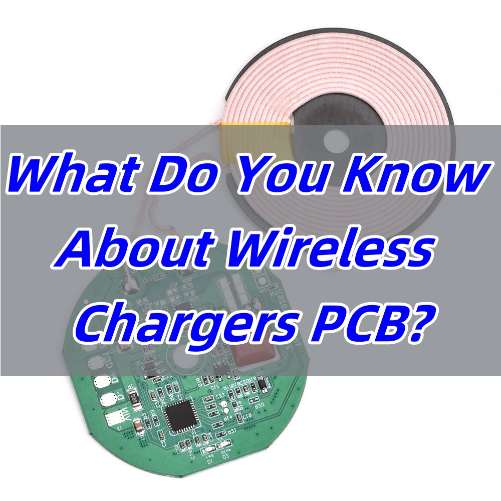
Wireless chargers PCB is increasingly important, which is driving the convenience of cable-free charging in modern devices. In today’s fast-paced world, wireless chargers have become an essential feature for many modern devices. At the heart of this technology lies the wireless charger PCB (Printed Circuit Board), which makes convenient, cable-free charging possible. If you’re interested in wireless charging technology, understanding wireless charger PCBs is key. At EBest Circuit (Best Technology), we specialize in the development and manufacturing of advanced wireless chargers PCBs that ensure high-performance charging solutions.

What Is a Wireless Charger PCB and How Does It Work?
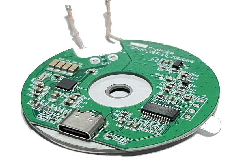
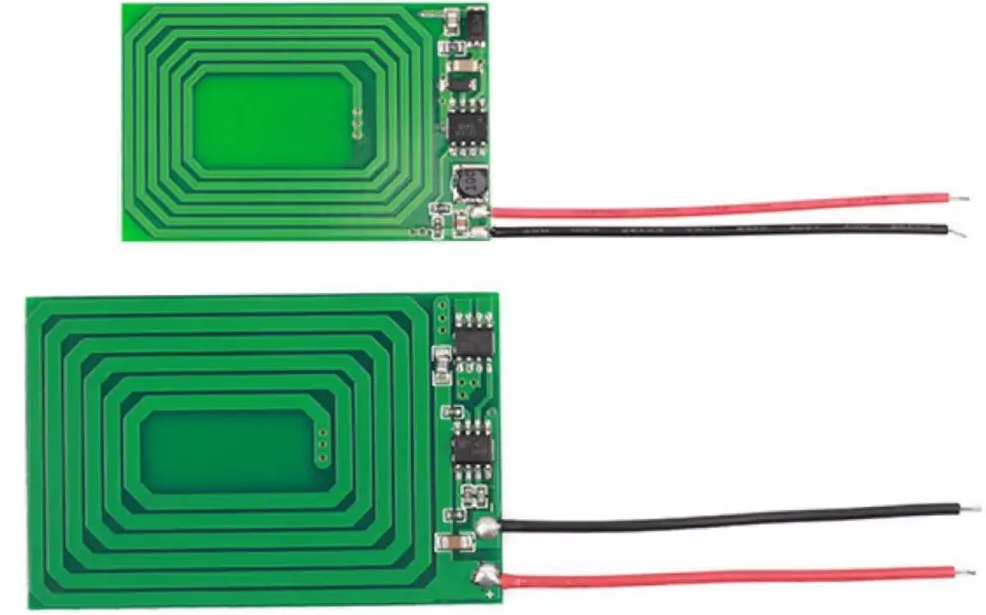
A wireless charger PCB is the foundational component that enables wireless charging in devices like smartphones, tablets, and wearables. At its core, it allows the transfer of power from the charger to the device without the need for physical connectors. The PCB acts as the conductor that integrates the coil and components required for energy transfer.
The system works using electromagnetic induction. When the charging pad is powered on, it generates an electromagnetic field. The coil in the wireless charger PCB picks up this field and converts it back into electrical energy to charge the device. This process is highly efficient, offering a seamless charging experience for users.
How to Design a Wireless Charger PCB?
Designing a wireless charger PCB requires careful attention to detail. There are several key aspects to consider:
Power Transfer Efficiency: The efficiency of power transfer is the top priority. Designers must carefully choose the right materials, size, and coil arrangement to minimize power loss.
Coil Design: The coil design directly influences how much power can be transferred. A larger coil area often results in higher efficiency. The PCB design must support optimal coil placement for maximum energy transfer.
Thermal Management: Wireless charging generates heat, so a good wireless charger PCB design incorporates heat dissipation strategies to prevent overheating, such as using thermal vias and heat sinks.
Electromagnetic Compatibility (EMC): Designers must also ensure that the PCB does not interfere with other devices. Shielding and proper grounding techniques are essential to prevent electromagnetic interference (EMI).
A skilled designer will take all of these factors into account, ensuring the wireless charger PCB operates smoothly, safely, and efficiently.
What Are the Benefits of Using Wireless Charger PCBs in Consumer Electronics?
Wireless charger PCBs offer numerous advantages, making them a sought-after solution for consumer electronics:
Convenience: With no cables to plug in, users can simply place their device on the charging pad. This eliminates the hassle of searching for cords or worrying about wear and tear on charging ports.
Durability: Since wireless chargers eliminate physical connectors, the wear and tear on ports is minimized. This extends the lifespan of devices, offering a more durable and reliable solution.
Aesthetic Appeal: Wireless charging pads can be seamlessly integrated into modern designs without the need for visible ports. This creates a more streamlined, aesthetically pleasing look for devices.
Safety: Wireless charging is often considered safer, as it reduces the risks of physical damage to connectors, as well as potential electrical hazards like short circuits.

What Are the Challenges in Wireless Charger PCB Design and How to Overcome Them?
While wireless charger PCB design has its benefits, there are also challenges to navigate:
Heat Generation: Wireless chargers generate more heat compared to traditional wired chargers. To combat this, designers must implement effective cooling mechanisms, such as thermal vias, heat sinks, or using materials with high thermal conductivity.
Size Limitations: The larger the coil in a wireless charger PCB, the higher the energy transfer efficiency. However, this can lead to size constraints in compact devices. Careful design is needed to balance size with performance.
Interference Issues: The electromagnetic fields generated by wireless charging can interfere with other nearby electronic devices. Designers must be diligent about shielding, grounding, and placement to mitigate this problem.
Cost Efficiency: High-performance materials can increase the cost of manufacturing a wireless charger PCB. It’s essential to balance performance needs with cost constraints to create a competitive product.
By understanding these challenges and applying effective solutions, manufacturers can develop wireless charger PCBs that meet both performance and safety standards.
What Is the Wireless Charger PCB Design Trend for 2025?
Looking ahead, wireless charger PCB design is set to evolve with several exciting trends:
Faster Charging Speeds: As consumer demand for quick charging grows, wireless charger PCBs will be designed to support higher power levels, reducing charging time significantly.
Multi-Device Charging: Designers are exploring ways to enable wireless charger PCBs that can charge multiple devices at once, enhancing convenience for users with several gadgets.
Smaller Form Factors: With ongoing advancements in technology, we can expect wireless charger PCBs to become more compact, allowing integration into smaller devices and spaces.
Sustainability: Eco-friendly materials and energy-efficient designs are expected to play a larger role in the development of wireless charger PCBs, as sustainability becomes a major consideration for manufacturers.
These trends are set to improve both the performance and convenience of wireless chargers, making them even more attractive to consumers.
How Does Wireless Charger PCBA Affect Charging Speed and Efficiency?
The wireless charger PCBA (Printed Circuit Board Assembly) plays a critical role in determining how fast and efficiently a device charges wirelessly. The quality of the PCB and its assembly can directly impact the power delivery rate, which affects both charging speed and efficiency.
Power Conversion: A well-designed wireless charger PCBA ensures efficient conversion of AC to DC power. Any loss in this conversion process can slow down charging speed.
Signal Processing: Advanced PCBA designs incorporate smart circuitry to optimize power distribution, allowing for faster and more stable charging.
Heat Management: Efficient thermal management in the wireless charger PCBA helps maintain consistent charging speeds without overheating, which is crucial for long-term battery health.

What Is the Best Material for Wireless Charger PCB?
The choice of material in wireless charger PCB construction is crucial to its performance and longevity. Some of the most common materials include:
Copper: Known for its excellent conductivity, copper is often used for the power and signal traces on a wireless charger PCB.
Ferrite: This material helps concentrate the magnetic field and improves power transfer efficiency. Ferrite is often used as a core material for the charging coils.
Ceramics: For certain high-performance applications, ceramics are used for their thermal stability and low electrical losses.
Choosing the right material depends on the specific needs of the design, including factors like efficiency, cost, and intended use.
How to Choose a Supplier for Wireless Charger PCB and PCBA Needs?
Choosing the right supplier for wireless charger PCBs is a crucial decision. Here are some factors to consider:
Experience and Expertise: Look for a supplier with a proven track record in designing and manufacturing wireless charger PCBs.
Customization Options: A good supplier will offer customization options to tailor the wireless charger PCB to your specific requirements, ensuring optimal performance for your devices
Quality Control: Ensure that the supplier has robust quality control measures in place to ensure the reliability and longevity of their PCBs.
Cost and Lead Time: Compare pricing and lead time across multiple suppliers to find the best balance of cost-efficiency and timely delivery
As the demand for wireless charging continues to grow, understanding wireless charger PCBs becomes more important than ever. By mastering the design considerations, materials, and emerging trends in wireless charger PCB technology, manufacturers can offer solutions that meet both consumer expectations and industry standards. At EBest Circuit (Best Technology), we specialize in creating high-quality wireless charger PCBs that ensure fast, efficient, and safe charging for your devices. Whether you are looking for custom designs or off-the-shelf solutions, we are here to help you meet your wireless charging needs with the best in class technology.


