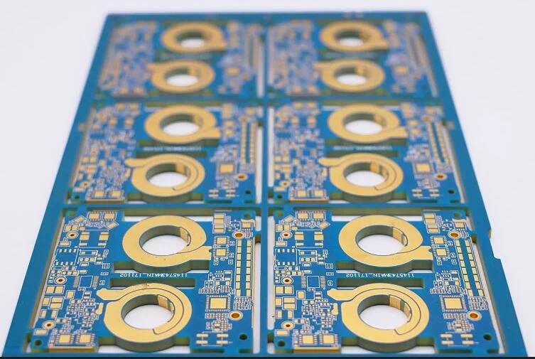
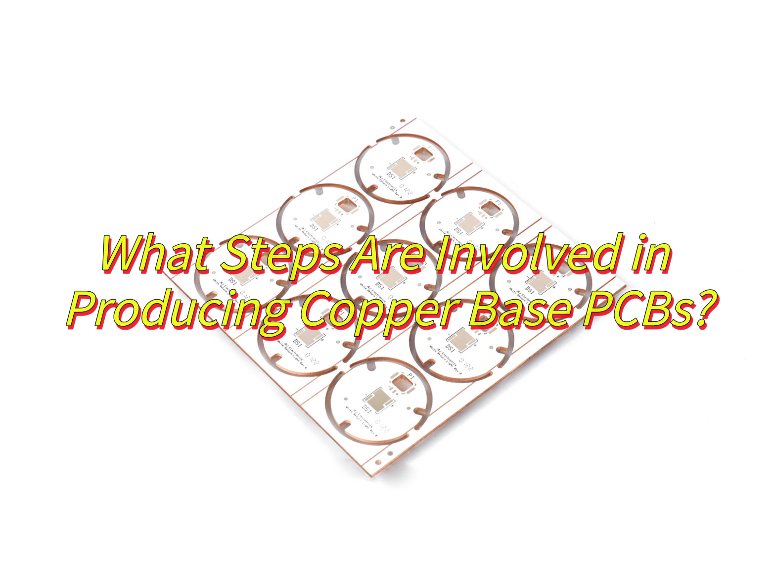
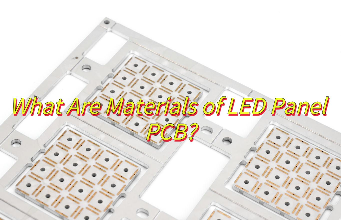
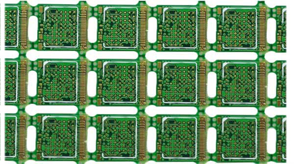
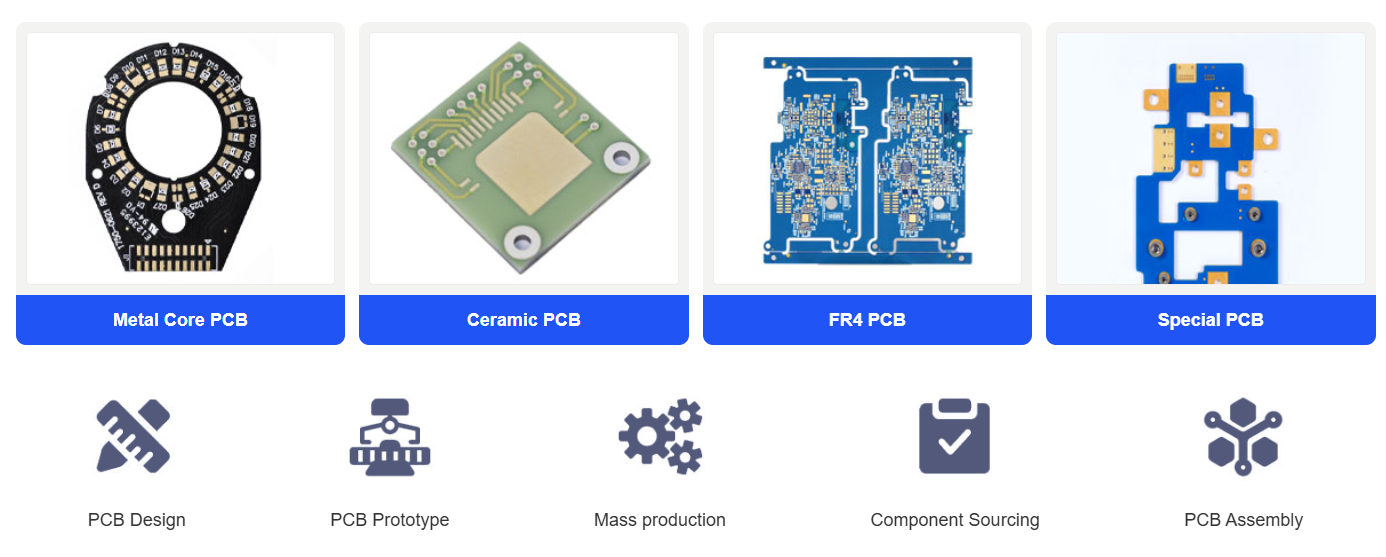
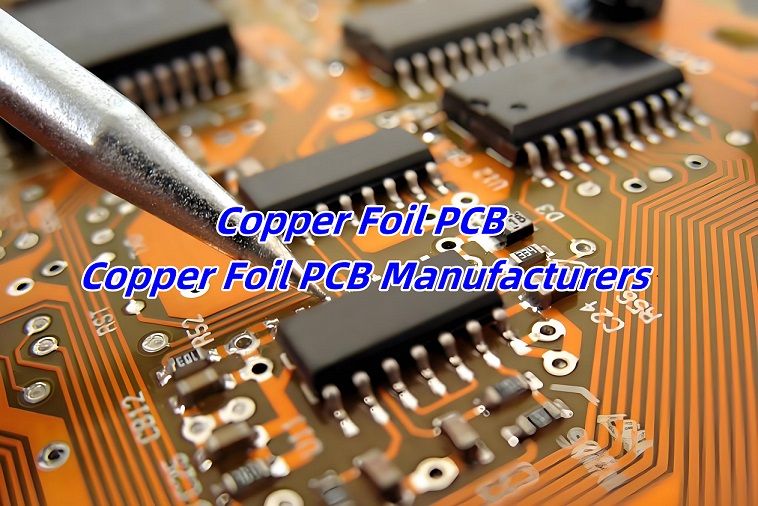
What is Copper Foil PCB?
A copper foil PCB is a type of printed circuit board where copper foil is laminated onto the base material to form the conductive layer. This copper layer is what carries electrical signals and power between different parts of the board. Without it, a PCB wouldn’t function at all.
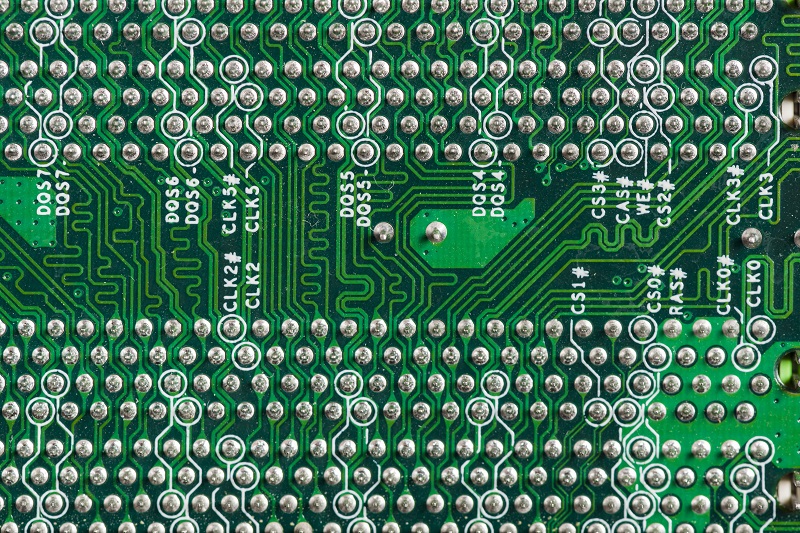
The copper is typically applied through lamination, where thin sheets of copper foil are bonded to a substrate, usually made of fiberglass-reinforced epoxy resin like FR4. This copper layer is then etched to create precise paths, known as traces, that connect components across the board.
There are also different thicknesses of copper foil used, which affect the board’s ability to carry current and dissipate heat. The standard thickness is usually 1 oz/ft² (about 35μm), but heavier copper options like 2 oz or 3 oz are often used in power electronics or high-temperature applications.
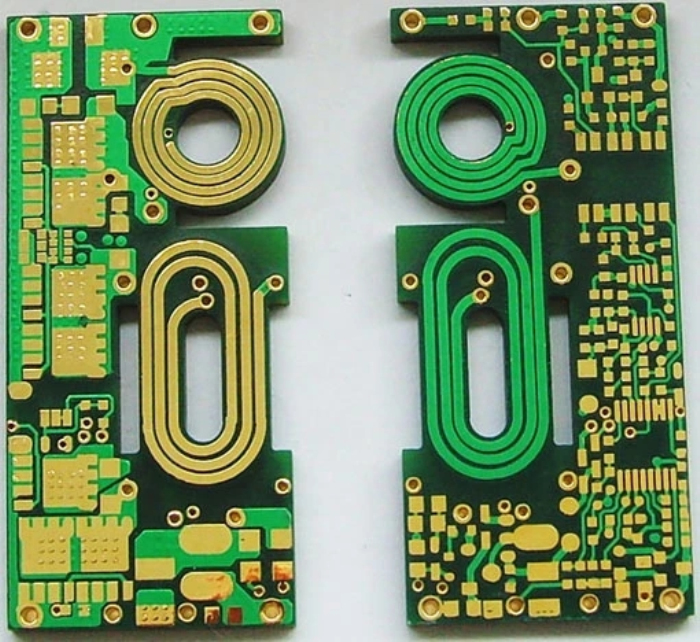
What is the Purpose of Copper Foil in PCB?
The main role of copper foil is to carry electric current across the circuit. It’s the path for data, signals, and energy. Without copper foil, there would be no communication between components.
Besides that, copper foil helps in thermal transfer. When current flows, heat is generated. Copper helps in spreading this heat evenly, reducing hot spots. That’s key in designs with dense parts or power-hungry chips. Also, copper layers add mechanical strength to the board, supporting solder joints and reducing flex.
What are the Different Types of Copper Foils?
Copper foil types vary based on how they’re made, how rough they are, and what kind of performance they offer in real PCB applications. Choosing the right type can make a big difference in signal clarity, layer adhesion, and long-term reliability. Let’s see the most common types used in the PCB industry:
1. Electrodeposited (ED) Copper Foil
Electrodeposited copper foil is the most widely used type in standard rigid PCBs. It’s made through an electrochemical process where copper ions are deposited onto a rotating stainless steel drum. The side in contact with the drum becomes smooth, while the other side is naturally rough.
ED copper foil is great for multilayer rigid boards, consumer electronics, and automotive circuits. When treated with surface chemicals, it bonds well to laminates and resists layer separation.
2. Rolled Annealed (RA) Copper Foil
RA copper foil is made by mechanically rolling solid copper into very thin sheets and then annealing it (heating and cooling) to relieve stress. You’ll find RA copper in flex circuits, flex-rigid PCBs, wearable electronics, and mobile devices. When boards must flex without breaking, RA is the go-to.
3. Reverse Treated Foil (RTF)
RTF is a type of ED foil where the shiny side is treated instead of the rough side. This treatment adds micro-etching or chemical bonding to enhance adhesion between the copper and the laminate. RTF is popular in HDI (High-Density Interconnect) boards, high-speed digital circuits, and RF designs where signal loss must be controlled.
4. Very Low Profile (VLP) and Ultra-Low Profile (ULP) Copper Foils
These are smoother versions of standard ED foils, created to reduce conductor roughness. VLP and ULP foils are still electrodeposited, but they go through extra steps to minimize surface peaks and valleys. They are used in high-speed digital systems, data centers, 5G antennas, and any application where clean signal transmission matters.
5. High-Temperature Elongation (HTE) Copper Foil
HTE copper foil is a variant of ED copper, enhanced for high thermal and mechanical stress. It resists cracking under repeated heating and cooling cycles. HTE is preferred for automotive, power electronics, and multilayer PCBs that go through reflow soldering or see high current loads.
6. Resin-Coated Copper Foil (RCC)
RCC combines copper foil with a thin layer of resin. This resin bonds directly to the core without needing prepreg sheets, which simplifies the lamination process. Mainly in mobile phones, compact devices, or where thin layers and high accuracy are needed.
Here is a summary comparison table between them:
| Copper Foil Type | Strength | Flexibility | Smoothness | Signal Performance | Application |
| ED | High | Low | Moderate | Standard | Rigid PCBs |
| RA | Medium | High | High | Good | Flex PCBs |
| RTF | High | Medium | Treated | Excellent | RF, HDI |
| VLP/ULP | Medium | Medium | Very High | Superior | 5G, high-speed |
| HTE | Very High | Low | Moderate | Standard | Power boards |
| RCC | Low | Medium | High | Good | Thin mobile boards |
What is the Roughness of Copper Foil in PCB?
The roughness of copper foil on PCB refers to the unsmoothness of the copper foil surface, Copper foil roughness affects how well signals move through the board. In high-speed designs, surface texture matters a lot. Rough copper increases insertion loss. This weakens the signal and causes noise.
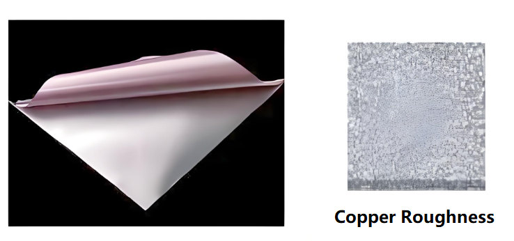
Roughness is usually measured in microns, which is usually quantified by Ra, Rz and Rq. Lower values are better for RF or high-speed data.
- Ra: The arithmetic average of the absolute value of the contour deviation over the sampling length, applicable to copper foil surface.
- Rz: Sum of the average of the 5 largest profile peak heights and the average of the 5 largest profile valley depths over the sampling length for copper foil rough surface.
- Rq: Means RMS (Root means square) value, it also is a roughness index.
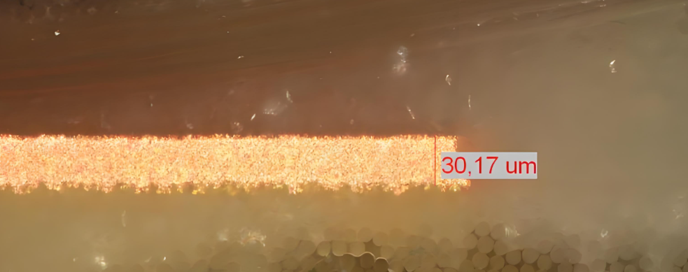
PCB Copper Thickness Chart
Copper thickness is often given in ounces per square foot. But that doesn’t mean much until you convert it. Here’s a helpful chart:
| Copper Weight (oz/ft²) | Thickness (µm) | Thickness (mil) |
| 0.5 oz | ~17 µm | ~0.67 mil |
| 1 oz | ~35 µm | ~1.37 mil |
| 2 oz | ~70 µm | ~2.74 mil |
| 3 oz | ~105 µm | ~4.11 mil |
| 4 oz | ~140 µm | ~5.48 mil |
- For single & double sided PCB, the copper foil thickness is about 35um, 50um, 70um;
- For multi-layer PCB, its outer layer copper thickness is 35um, and inner layer copper thickness is 17.5um (1/2oz).
Designers choose copper weight based on current flow and thermal limits. Thicker copper is used in power PCBs. Thinner layers are more common in signal circuits or HDI boards.
HTE vs RTF copper foil
When it comes to choosing the right copper foil for high-performance PCBs, HTE (High-Temperature Elongation) and RTF (Reverse Treated Foil) are two of the most commonly used options.
- HTE Copper Foil
HTE copper foil is a specially processed electrodeposited foil that’s engineered to handle high thermal and mechanical stress. The term “high-temperature elongation” refers to the foil’s improved flexibility and stretch resistance when exposed to heat.
It’s treated chemically to improve adhesion strength, making it more reliable during multiple soldering cycles. The surface has a consistent profile that bonds well with different dielectric materials.
Key Features of HTE Foil:
- Strong peel strength
- Durable under repeated heating
- Excellent for plated-through-hole (PTH) reliability
- Withstands lamination and solder reflow cycles
- RTF Copper Foil
RTF, or Reverse Treated Foil, is also made through an electrodeposition process, but with one key difference: the shiny side gets treated instead of the rough side. This treatment applies a fine, uniform microstructure that enhances bonding without creating high surface roughness.
This smoother surface makes RTF a preferred option in high-speed signal and RF PCB applications where low signal loss is critical.
Key Features of RTF Foil:
- Lower surface roughness
- Better electrical performance at high frequencies
- Improved signal integrity
- Balanced peel strength and performance
PCB Copper Electrical Conductivity
Copper has one of the highest electrical conductivities of any metal. That’s why it’s the go-to choice for PCBs. The typical conductivity of copper used in PCBs is about 5.8 x 10⁷ S/m (Siemens per meter).
This high conductivity allows small traces to carry high current with low voltage drop. It also reduces signal distortion, which is key in high-speed or RF applications.
Still, conductivity depends on purity. Most PCB foils use 99.9% pure copper. If copper is oxidized or poorly handled, conductivity drops. That’s why clean processes and proper lamination are important.
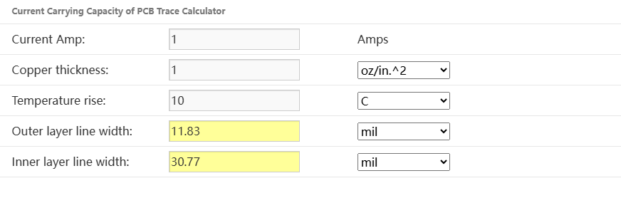
How to Calculate Copper Thickness in PCB?
The thickness of copper in PCB can be calculated by the following methods:
1. Calculation of copper plating thickness by current density and plating time:
Plating thickness (um) = current density (ASF) x plating time (min) x plating efficiency × 0.0202. This formula takes into account the amount of electricity, equivalent, molar mass, density and other factors. The specific calculation process involves the product of current density, plating time and plating efficiency, then multiplying by a factor 0.0202.
2. Thickness calculated by weight of copper foil:
In the common option “copper-covered FR4, single-sided,1 oz”,1 oz indicates the thickness of the copper foil. 1 oz = 28.35 g/ft², copper foil density of 8.93 g/cm³, 1 square foot = 929.03 cm². Thus, 1 oz copper foil thickness = 28.35/8.93/929.03 ≈ 35um or 1.35mil . Common PCB thicknesses include 1/2Oz = 17.5um, 1 oz = 35um, 2oz = 70um, and 3 oz = 105um.
In addition to these two methods, you can also use our online pcb copper thickness calculator to calculate the copper thickness.
Copper Foil PCB Manufacturers
Many trusted copper foil PCB manufacturers serve global markets. Some of the top names include:
1. Isola Group: Known for high-frequency and low-loss materials.
2. Kingboard: One of the world’s biggest copper clad laminate suppliers.
3. Ventec International: Offers low-profile copper foils and thermal substrates.
4. Mitsui Mining & Smelting: A top name in RTF and ultra-smooth foils.
5. Best Technology: Based in Asia, with 18+ years in the industry. We supply high-quality copper foil PCBs, from 0.5 oz to over 6 oz.
At Best Technology, we bring over 18 years of hands-on experience. We support standard and custom copper weights, including heavy copper for high-current boards. Our RTF and HTE options fit both signal-sensitive and power-heavy needs.
With fast lead times, in-house testing, and global delivery, we’re more than just a PCB maker. We’re your reliable partner for copper foil PCB solutions. Reach out today to explore your next project with confidence.