Via hole wall thickness is determined by the plating normally 1/2 OZ or 1 OZ is used based on your design application. Power boards will go for more Ounces.
For power signal via – it’s important to consider the current, temperature rise in PCB, plating, PCB material used.
According to IPC-6012, the standard via hole wall thickness is 15-18um. But Best Tech can make via wall with 40um.
If the hole copper thin, resistance, and wide current, fever, high temperature, especially in SMT and wave soldering) base material resin (high expansion coefficient) is prone to mechanical stress of hole copper, and the thermal stress, pore copper prone to mechanical fatigue, hole wall with micro cracks. There may be holes separation of copper and the inner pad.
It is a 2 layers stack up including via holes, and you can find the via wall details. BTW, there are via wall just when we do Plated Through Hole to connect Top layer and bottom layer.
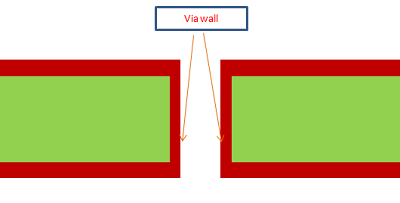
Via wall on PCB
Tags: via wall


