pcb
Home > Blog

Archive for August, 2016

What is the PCB flying probe test?
Friday, August 12th, 2016

Flying probe test is a check PCB electric function method (one of the short circuit test). Flying probe tester is for component layout density, layer number, wiring density, small distance of measuring points of PCB (printed circuit board), a kind of testing instrument, the insulation of the main test circuit board and conduction values.

The advantages include: rapid test development; Low cost test method; Fast conversion flexibility; and in the prototype stage for designers to provide rapid feedback.

The disadvantages include: Because of easy programming, to within a few hours test prototype assembly, and test the low yield of UUT without typical fixture development costs, flying probe test can solve many problems in production environment. But not all production test problem can be solved by using the probe automatically.

You may also like

Through Via
Friday, August 12th, 2016

This is also one of the simplest holes, because when production as long as the use of bit or laser light directly do circuit board drilling, all costs are relatively cheap. Through vias are the oldest and simplest via configurations originally used in 2-4 layer PCB designs. Since the signals originate and terminate from the outer layers of the PCB, there are no stubs. In multi-layer PCB applications, they are an inexpensive way to eliminate the resonance effects caused by stubs where other mitigation techniques are not practical or are too expensive.

Vias make electrical connections between layers on a printed circuit board. They can carry signals or power between layers. For backplane designs, the most common form of vias use plated through hole (PTH) technology. They connect the pins of connectors to inner signal layers. A PTH via is formed by drilling a hole through the layers to be connected and then copper plating it.

You may also like

Difference for normal TG and high TG?
Friday, August 12th, 2016

General Tg board for more than 130 degrees, high Tg generally greater than 170 degrees, medium Tg is greater than 150 degrees.

Usually TG of 170 ℃ or more PCB PCB, called high TG PCB.

When increases TG for the substrate, the PCB board cane withstand heat resistance, moisture resistance, chemical resistance, resistance to stability characteristics will improve and enhance. The higher the TG values, plate temperature resistant performance is good, especially in the lead-free process, high TG application is very popular. High TG means high heat resistance.

The difference for normal TG and high TG is:

under the hot circumstance, especially after moisture absorption heat, its material mechanical strength, dimensional stability, adhesion, water absorption, thermal decomposition, thermal expansion differences between various conditions such as high Tg products bright sun better than ordinary PCB substrate material.

You may also like

PCB solder mask ink
Friday, August 12th, 2016

PCB solder mask ink

PCB solder resist ink is mainly used in circuit board, also called PCB inks, prevent short circuit caused by soldering pulling, at the same time it also has excellent Electrical Performance, Chemical performance. Moisture proof, mould proof, salt fog resistance.

PCB solder mask ink main functions are as follows:
(1)Prevent physical disconnection of the circuit conductors;
(2)Welding process, to prevent short circuit because of the bridging;
(3)Only in part must be welding welding, to avoid solder waste;
(4)Reduce copper pollution of welding groove;
(5)To prevent from dust, moisture and other external environment factors causing deterioration of insulation, corrosion;
(6)High insulation, made it possible to high density change of the circuit。

You may also like

The function advantage of the PCB
Friday, August 12th, 2016

The board of the PCB itself is by the material of insulation and heat insulation, and is not easy to bend into. PCB appearance and development of the unique features of the printed circuit board, brought significant reform to the electronics industry, greatly promote the upgrading of electronic products. This is because the printed circuit board PCB has many unique functions and advantages:

See following tips:

  1. Printed circuit board PCB is a good consistency, it can be used in a standardized design, conducive to the production of automation and mechanization of welding equipment, improve the productivity.
  1. Printed circuit board PCB equipment parts have good mechanical properties and electrical properties, make electronic equipment unit combination, make the whole piece after assembly and debugging of printed circuit board as spare parts, is advantageous for the whole products swaps and maintenance. It is because of the above advantages of PCB, printed circuit board PCB has been very widely used in the manufacture of electronic products, without a printed circuit board PCB, there is no rapid development of modern electronic information industry. Familiar with the basic knowledge of printed circuit board PCB, master the basic design method and the printed circuit board PCB production process, understand the production process is the basic requirement of electronic technology study.
  1. Printed circuit board PCB advantage is to achieve electrical connection between the various components in the circuit, instead of the complex wiring, reducing the workload of traditional mode of connection, simplifying the electronic products assembly, welding, commissioning work.
  1. Printed circuit board PCB is narrowed the equipment volume, reduces the product cost, improve the quality and reliability of electronic equipment.

You may also like

Why the PCB have test point?
Friday, August 12th, 2016

The test point is designed to test the components of the PCB if they meet the specifications and solder mask or not. For example, if we want to check a resistance on the circuit board if have any problem, the easiest way which is use the universal meter to measure the both ends of PCB. But if there have a large number of PCBs, it is hard to use the universal meter to test each components are correct or not one by one. So we can use the automated test machine of ICT(In-Circuit-Test) to test, which is designed by probe (normally called “needle Bed (Bed – Of – Nails)” fixture). This test machine can test all the circuit of components on the PCB at the same time. Then through the way of program control to measure the characteristics of the components. Generally speaking, the PCB only need to take around 1-2 minutes to finishih the testing. The testing time are depending on the components’quantity, the time will be more longer with the more components.

But if the probe contact with the components or solder pads on the PCB directly, it will damage some components easily. So the engineers design the “test point” on the PCBs, which is designed the additional parts to elicit a pair of round on the both ends of components, and there is no solder mask. It can contact these small test points directly and measure the components by the probe.

You may also like

Generally speaking, the hole of PCB have PTH, blind via hole and buried hole.
Friday, August 12th, 2016

Generally speaking, the hole of PCB have PTH, blind via hole and buried hole.

One of the most common is Plating Through Hole (PTH),  the criteria of judging whether the hole is PTH, you can focus the PCB on the lamp, the light hole is PTH. During production, it can use the drill or laser to drilling the hole of PCB. So it is the most simple tpye of hole, and the cost are more cheaper than onters. But there also has some layer of PCB doesn’t need this hole, because it will take up some place of PCB.

The outermost layer of Blind Via Hole is connected to the adjacent inner’s plating hole, and the hole call “blind” since it can’t see the opposite. The production of blind hole is in order to make full use of space with the PCB circuit layers. This manufacture method should pay more attention to the depth(Z axis) of hole, almost no one in this way since the inner hole will be difficult to plate. And we can drill the hole of the connected circuit layer in advance when they in other layers and then stick up, but it needs  precision positioning and contrapuntal device.

The internal layers’ connection but without conducting any circuit layer to the outer layer of PCB, which called the buried hole. This process cannot be completed by the way of stick up the drilling hole, it has to drill the hole in each layer. After bonding inner layer, it needs to plate firstly and then stick up all layers. Since it will spend more time to process than the PTH and Blind hole, so it will be more expensive. Finally, the production of buried hole just suitable for the HDI PCB, in order to enlarge the space of each layer for PCB.

You may also like

What’s the coverlay’s purpose and characteristics?
Friday, August 12th, 2016

The first purpose of coverlay is that cover and protect the FPC circuit, enhance the rupture resistance of FPC.

Secondly, keep the circuit away from the injury by temperature, humidity, pollution and Corrosive material.

Thirdly, to cover the follow-up surface finishing of the FPC.

What’s more, it has the effect of soldermask in FPC SMT.

And the first characteristics of coverlay, it is suitable for the traditional way and rapid pressing on the same time.

Secondly, the heat resisting property and peel strength can keep a long time.

Thirdly, it can control the glue squeeze-out.


The coverlay still has the excellent bending resistance, it is suitable for the high flexible FPC.


And it meet the requirement of RoHS, the coverlay does not contain lead, mercury, cadmium,Polybrominated biphenyls,polybrominated diphenyl ether and red phosphorus.

You may also like

How do we ensure quality?
Friday, August 12th, 2016

Our high quality standard is achieved with the following.

  • The process is strictly controlled under ISO 9001:2008 and IPC-A600/IPC-A610 standards.
  • Extensive use of software in managing the production process
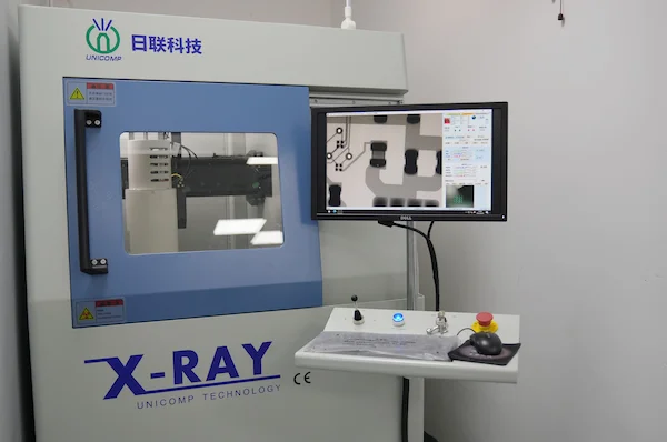
  • State-of-art testing equipments and tools. E.g. Flying Probe, X-ray Inspection, AOI (Automated Optical Inspector) and ICT (in-circuit testing).
  • Dedicated quality assurance team with failure case analysis process
  • Continuous staff training and education

You may also like

what is the goods insurance during the international transportantion?
Friday, August 12th, 2016

In order to delivery the cargo security to the consignee, avoid the damage, loss,
especially for the a large high value goods, insurance is the required.

For the air and sea cargo, usually we buy the insurance from
CHINA PACIFIC PROPERTY INSURANCE CO.,LTD.

It includes the insured, B/L No. quantity, name, amount Insured,transportation,
date, route,Deductible and Claim payable so on.

The amount Insured should be 110% of the actual goods value.
DEDUCTIBLE usually is USD200.00 OR  5% OF THE LOSS,WHICHEVER IS THE GREATER.

You may also like