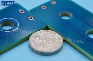
The advantage of the blister packaging.
Normally we pack the goods use PP bags, red bubble film and PE foam, they can protect well the goods.
But when we do the SMT, especially for the big bulge components, PE can’t protect well.
So need to do the blister packaging.
The advantage is can pack any kinds of grotesque goods well, save materials, light weight, easily shipment,good sealing,ROSH, no need to add other buffer material.