
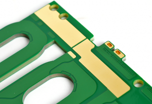
According to the new definition within IPC-T-50M a micro via is a blind structure with a maximum aspect ratio of 1:1, terminating on a target land with a total depth of no more than 0.25mm measured from the structure’s capture land foil to the target land.
Archive for August, 2016
Friday, August 12th, 2016

Friday, August 12th, 2016
Yes, in general, if you need the copper base thicker, the wider the track should be. One rule of thumb is that with a 18 µm copper base the track should not be narrower than 0.1 mm (4 mil) and with a 105 µm copper base the track should not be narrower than 0.25 mm (10 mil).
You may also like
Friday, August 12th, 2016
The answer is no, BT layer (Like as the FR4) and dielectric layer are very important, it is impossible to skip both of them or one of them.
Because the copper can’t be combined with meatal core, if we remove them, then we can’t make the trace on the metal base.
The other reason is the dielectric layer is most important for heat dissipation, normally, dielectric layer the thicker the better.
You may also like
Friday, August 12th, 2016
Please let me know what is the minimum via size and the minimum copper diameter around the via.
1) The minimum via size means the minimum diameter for the PTH (Plated Through Hole) or NPTH( Non-Plated Through Hole).
Normally, for MCPCB, the minimum diameter of PTH is 0.3mm, the NPTH is 0.25mm.
2) The meaning of the minimum copper diameter around the via is hole ring.
Normally, the minimum diameter of hole ring is 0.2mm.
You may also like
Friday, August 12th, 2016
No, it is not always. There are many factors to be taken into account, e.g. how many layers, the thickness of the PCB and also a good understanding of the assembly process (number of soldering cycles, time above 260 degrees, etc.). Some research has shown that a material with a “standard†Tg value has even performed better than some materials with a higher Tg value. Note that even with “leaded†soldering the Tg value is exceeded.
What is of most importance is how the material behaves at temperatures above the Tg value (post Tg) so knowing the temperature profiles the board will be subjected to will help you look evaluate the necessary performance characteristics.
You may also like
Friday, August 12th, 2016
The relationship between the diameter of the hole and its length. When a manufacturer states that their production has an “aspect ratio†of 8:1 it means, for example, that the hole’s diameter is 0.20 mm in a 1.60 mm thick PCB.
For HDI structures, a suitable aspect ratio for micro via is normally 0.8:1, with 1:1 preferable for ease of plating.
You may also like
Friday, August 12th, 2016
Normally working temperature of MCPCB is <130℃, better less than 100C, dielectric layer in MCPCB is the bottle neck for high temperature, as the Tg value of that layer is only 130℃
Ceramic PCB can be: -50℃ to 800℃.
So if temperature higher than 130℃, then Ceramic PCB or High Tg PCB (but only around 170C) is good choice.