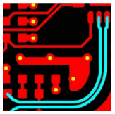
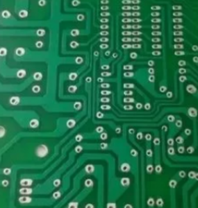
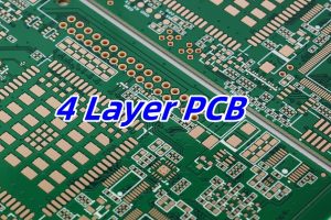
This is also one of the simplest holes, because when production as long as the use of bit or laser light directly do circuit board drilling, all costs are relatively cheap. Through vias are the oldest and simplest via configurations originally used in 2-4 layer PCB designs. Since the signals originate and terminate from the outer layers of the PCB, there are no stubs. In multi-layer PCB applications, they are an inexpensive way to eliminate the resonance effects caused by stubs where other mitigation techniques are not practical or are too expensive.
Vias make electrical connections between layers on a printed circuit board. They can carry signals or power between layers. For backplane designs, the most common form of vias use plated through hole (PTH) technology. They connect the pins of connectors to inner signal layers. A PTH via is formed by drilling a hole through the layers to be connected and then copper plating it.


