What is via?
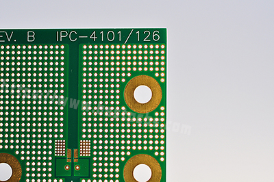
A via plays an important role in multi-layer PCBs. It is used to make an electrical connection between the layers of a multi-layer PCB. Generally speaking, every hole in the printed circuit boards can be called as via.
A via is constructed by placing copper pads on each layer of the PCB and drilling a hole through them. And the hole is plated with copper that forms electrical connection through the insulation that separates the copper layers.
Types of Vias
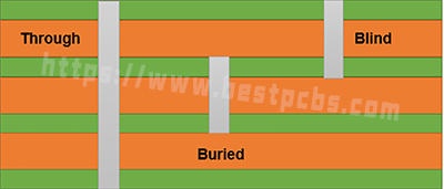
There are three main types of vias used in PCB: through-hole via, blind via and buried via.
Through-Hole Via
Through-hole via goes right through the printed circuit board from top to bottom and can be used to connect all the layers of a PCB. It is the most common via and is easiest to construct.
Blind Via
Blind via connects the outermost layer of a PCB to the next layer. Namely, it cannot be seen on the other side of the board and is therefore called blind via.
Buried Via
Buried via is used to connect internal layers of a PCB. And it cannot be seen on the surface of the board.
In addition, it is always better to use multiple smaller vias rather than one large via since smaller vias can reduce the inductance and also provide an additional path to the current flow in case any of the vias fail.
So, this is the end of this article. In case if you have any questions, you are welcome to contact us via email at sales@bestpcbs.com. We are fully equipped to handle your PCB manufacturing requirements.
Tags: PCB


