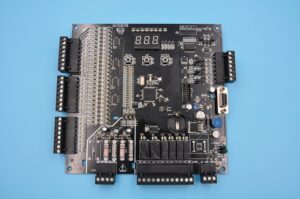
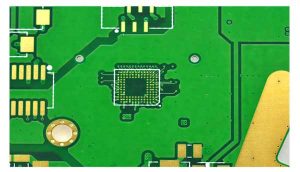
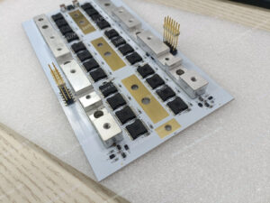
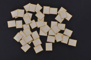
We know due to the rapid development of electronic devices, Ceramic circuit boards have gradually developed into an ideal packaging substrate for a new generation of integrated circuits and power electronic modules. Among them, thick film ceramic substrate and thin film ceramic PCB are the most popular ceramics that be used in package, because they are made by metallization process.
Why use film technology?
Compared with three-dimensional ceramic materials, film has relatively thin thickness and small size, it can be regarded as a two-dimensional structure. Thick film is made by printing process, the thick film can be made independently and the thickness is usually 10~25μm. Thin film is formed by the composition of the conductor materials and it was sputtering on the ceramic substrate directly. Normally the thickness of thin film is equal or less than 1μm. If the metallization thickness between 1μm to 10μm, then we called it as Directly Plated Copper (DPC) ceramic circuit board.
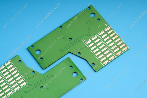
Thick Film Technology
Thick film technology is a method of direct deposition of slurry on substrate through screen printing technology, and sintering at high temperature to form conductive traces and electrodes. After the material is sinter at high temperature, it will form a strong adhesion film on the ceramic circuit board, and after repeated many times, it will form a multi-layer interconnected ceramic circuit board with resistor or capacitor. The thick film manufacturing process is more easier than thin film.

Thin Film Technology
Thin film ceramic PCB is a chip manufacture technology, which is the main method of metal film deposition in microelectronics fabrication. It was made through evaporation and PVD process firstly to deposited a 200-500nm copper layer as the seed layer. Then using electroplating process to increase the copper foil to required thickness. Finally through stripping and etching to generate the circuits. Thin film ceramic circuit is widely used in LED package fields because its fine traces, high accuracy and heat dissipation.

Thin film and Thick film ceramic PCB comparison
In addition to the technology manufacturing difference, their performance and limitations also is different. Here we summarized in below table:
| Technology | Thick Film | Thin Film |
| Conductor thick | 10-25um | <=1um |
| Manufacture process | Screen printing, sinter | PVD, DES |
| TCR | (50-300) *10-6/C | (0-50) *10-6/C |
| Cost | Relatively Low | High for prototype |
| Line width | Thicker line width | Fine traces, suitable for RF |
| Bonding ability | Not suitable for bonding | Good for wire bonding |
| Resistance | Available | Need mount resistors |
| Solder mask | Available | Available |
Application difference between Thin film and Thick film ceramic PCB
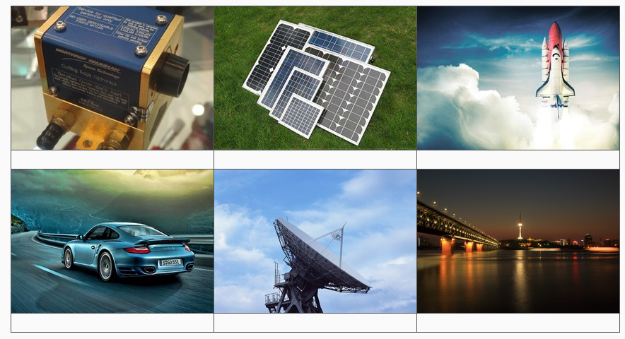
The applications of thin film and thick film also are different because of their different features. Thick film ceramics are widely used in high power devices such as automotive field, power electronics, aerospace due to its ability to handle high current and voltage. Thick film enables to provide excellent thermal management and can dissipation heat effectively. Thin film ceramic PCBs trend to micro-electronics and RF devices because of its fine lines, low resistance, and high-frequency performance.
Each technology has its unique advantages and limitations, it needs to be properly used to make it suitable for different electronic devices and industries. Choose the right ceramic PCB substrate for laymen is a big challenge, so seeking for a reliable supplier is important. Best Technology engaging ceramic circuit board manufacturing for over 10 years. And our core engineering team are deep in this industry for more than 20 years, we are so confident that we can provide the best solution for you. If you are interested in this, welcome to contact us at sales@bestpcbs.com.
Tags: thin film ceramic pcb


