pcb
Home > Blog

Archive for October, 2023

How Can I Reduce and Optimize the Cost of My PCB in A Best Way? – Series 2
Saturday, October 28th, 2023

At our latest blog, may the readers have understood the factors that will affect the PCB price, or maybe one of your have put it into practice that get a price lower than your budget. However, people are always not satisfied by the existing situation. If this is bother you as well, keep reading since this time we are going to sharing some useful tips that enable to optimize your PCB price until to the best.

  • Reduce board complexity

It can be said that try to simplest your design/layout and make it easy to fabricate is the simplest way to reduce your PCB cost. The more complex and irregular the forms, the higher the cost. Just remember: for every circuit board, no need to maintain a fancy diagram to demonstrate its excellence, perform functionality correctly is enough.

  • Design it in right size and thickness

Design your board in right size doesn’t means make it smaller as possible. You must know, if your design is complex and layouts are density, that means maker need to spend more time to assemble them. Highly compact sizes are always expensive, don’t skimp when it counts. Otherwise, more money will be spent to afford what you saved.

And in theory, the more layers and thickness the board, the more cost that manufacturer spend. Numerous layers in the PCB will have an influence for holes and diameters. It is recommended that if thinner thickness is enough, then just do it. 

  • Shapes, holes and rings should be regularly

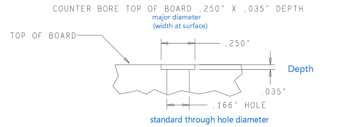
Normally, keep the PCB as square or rectangular shapes is cheaper than irregular shapes like pentagon.  And large holes and rings enable to smooth the production run and easy to create. For smaller holes and rings means the driller must be smaller and delicate control.

  • Consider volume and choose manufacturer

In our last blog, we emphasize manufacturers will set a minimum order quantity (MOQ), it is common in this industry. So, consider your volume and check multiple quantities before ordering can help to recognize which one is the most cost-effective.

During the evaluation period, talk to your suppliers as soon as possible, knowing more about the material specifications, technical and PCB tolerances. A wrong choice will lead to much time waste and some unnecessary cost. This is we call “trial and error cost”. Try to make all things are clear and correct before production.

  • Pick the best vias

There are totally three types of vias in PCB: though-hole, blind, buried. The through hole can be passed through the whole board, while blind vias is created from top or bottom side to the middle of the board without through to bottom or top side. Buried vias, just as its names, it is buried inside the boards and we can’t see it by naked eyes.

Obviously, through hole is cost performance than other two vias, try to use more instead of blind or buried vias enable to decrease your cost. In additionally, blind and buried vias are always necessary in HDI PCB and RF board, otherwise, you don’t usually use them.

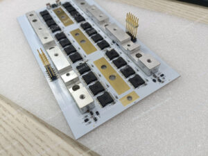
  • Make sure all SMT components on the one side

Trying to make all the surface mounted (SMT) components on the one side of circuit board if possible. In this way, assembler can finish the SMT process in one-time, so that can save much manufacturing time and cost. But if the components are distributed on both sides, it is needed to assemble two times, that is top side first – bottom side second (or sometimes bottom first).
  • Select easily replaceable component parts

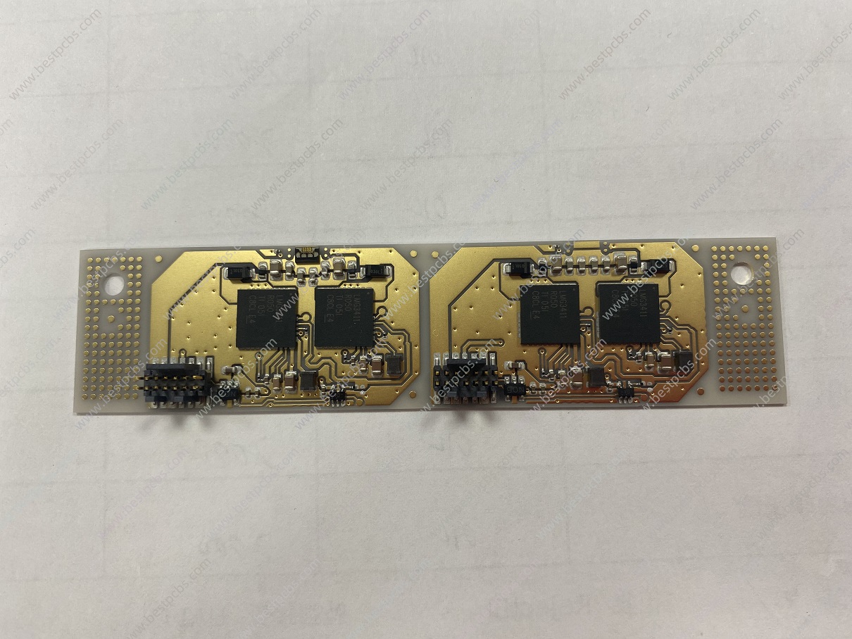
It is assumed that one of part on your circuit becomes obsolete, then you must search for replaceable part or update your design if you would like to continuedly use this board. As an extensive experienced PCB manufacturer, we strongly recommend that select components that has standard dimension, so that it is easy to match alternative one.

In addition, visit some manufacturer’s website carefully to see if any components are marked as “obsolete” or “not recommended for new designs” before finishing your design. This enables to avoid secondary update.

  • Follow manufacturer’s PCB fabricate standards

Understand and follow manufacturer’s fabricate standards can keep your unit PCB price in a relative lower cost. When designing a new project, please make sure to following below tips.

  1. Use standard stack-up with standard materials.
  2. Design 2-4 layers PCB if possible.
  3. Keep your minimum line width and spacing within the standard spacing.
  4. Avoid adding extra special requirements as much as possible.
  • Use SMT components as possible

Choose surface mounted (SMT) components instead of through hole (THT) component whenever possible. SMT and THT are almost treated as separated manufacturing processes. Hence, if all the THT components can be replaced by mounted parts, the THT process will be eliminated completely. It is not only decreasing the manufacturing cost, but also reducing delivery time. Of course, it is not always possible, but it’s worth trying.  

Whatever decisions you make, the best solution is to consult and discuss with your suppliers. They be always to give you the best one that can save your money and meet your requirements as well. Meanwhile, if you don’t believe the suppliers, you are welcome to reach us. We promise that we can give you a most favorable price and high-quality product.

You may also like

What Factors Affect the PCB Board Price? How to Keep the Best Price? – Series 1
Saturday, October 28th, 2023

For each development engineer or purchaser, how to keep the cost within the budget is a most irksome and irritating assignment while the PCB has the good quality and enable to perform desired function. They need to understand the computation rule and calculate the developing cost. So, it is worth to knowing the factors that affect the printed circuit board price, and it is a must learn course for every engineers. Herein, Best Technology is going to dissect the factors affect the cost of PCB, let’s move on!

What affects the cost of a PCB?

Drives the cost of PCBs are numerous, we can see from the PCB itself, for example, circuit board substrate materials, the external factors such as the manufacturing difficulties, the whole order quantities and some other special requirements that from designers.

Here, we listing some basic parameter factors which drives the whole cost of a PCB.

  • PCB substrate material

The substrate of PCB board refers to the material used in the non-conductor part of the circuit board, mainly FR4, glass fiber, epoxy resin, polyimide, copper, aluminum and so on. In the PCB manufacturing, glass fiber is widely used in the manufacture of double-sided circuit board and multi-layer board, while epoxy resin and polyimide are used in the manufacture of high-density multi-layer board. Among them, copper substrate is most expensive material. No matter what kind of materials, all of them shall be calculated according to the real-time international price.

  • PCB size (panel and single pcs)

PCB size will determine the price of PCBs, this is for sure. Generally speaking, with a same number of PCB layers, the smaller the PCB size, the cheaper the cost. Because during calculating cost, vendors will consider the utilization rate of raw materials. Make sure the highest utilization, the cost for both purchaser and vender will be best. The raw material of PCBs is commonly 1200mm*1200mm, or 1220mm for special specifications, when the utilization achieves 90% or above, this is the best.

So, how to improve the utilization of raw materials? Normally, manufacturers will optimize the working files (WF) from single size to panel size, and then material will be cut according to the panel files. But if the panel size is not suitable, then there will be a lot of waste edges of raw material in the cutting process, and generally this will be added into your PCB price. So that the unit PCB price will be more expensive. In another word, if you PCB size is well-suited, then it is good for PCB manufacturer and yourself. And at this time, the utilization will be the highest and your PCB cost is the cheapest as well.

  • Line width/spacing

To a certain extent, as long as you are following the PCB design rules, the PCB price will not too high. However, if your design is complex and the line width is extreme thin, then the price will increase since it is difficult to control during manufacturing.

  • PCB layers

According to the IPC standard, PCBs can be classified to single-layer PCB, double sided PCB and multilayer PCB. For layer count over than 2 layers, we called it as Multilayer PCBs, such as 4 layers PCB, 6 layers PCB. For FR4 PCB, we can make up to 32layers.

Due to the manufacturing process and some unpredictable assembling cycles, the more the layers, the more expensive it is. (The price of single side PCB is the similar to double sided PCBs.)

  • Solder mask ink color

In the past, it is no doubt that you will spend more if you want every color expect green. But now things are changeable. Most colors are available at no or very little extra cost, which usually only occurs for unique requests such as matte tones.

  • PCB copper foil thickness

The weight of copper foil depends on the successful utilization of the material. Thicker copper is more expensive and comes with additional manufacturing difficulties and expenses. You may also have to fill the holes with copper foil to connect layers. In addition, heavier copper means you need to spend more cost in shipping. Let’s take a simple example, for aluminum core PCB and copper core PCB, in the same volume and quantities, copper core PCB stands out for expensive shipping cost since it has thicker copper and heavier weight.

  • PCB surface treatment

Surface treatment is a method that using for protecting the surface from corrosion and improve the solderability. Usually, in consideration of environmental friendliness, vendors can use a couple of gold or silver to achieve further safety for use in some applications.

The commonly used surface treatment methods include OSP, IMMERSION SILVER, ENIG, ENEPIG and HASL (LF). Among them, the price is ENEPIG>ENIG>IMMERSION SILVER>OSP>HASL. You can calculate the PCB board price according to the surface treatment method and gold thickness.

  • Quantity and lead time

When developing a new project, almost of companies would like to make prototypes first and ask for a sample quotation. However, some PCB manufacturers will set the minimum order quantity, the smaller the quantity, the higher cost the PCB board. Please make sure to check the price for different amount before placing an official order.

Meanwhile, the delivery time request also will affect the whole price in a certain. And certainly, the price of quick turn order and expedited service will higher than normal order.

  • Other special requirements (impedance, IPC standard)

To ensure the stable transmission of circuit board signals and improve the quality of signal transmission, designers and engineers will ask for impedance control for the traces. This can be seen as special requirements, so it will add a few extra prices. And the required IPC Criteria is a factor as well. Normally, if customer does not have other request, we will default use IPC class II. III level will more expensive.

Above all are the mainly factors that affect the price composition for a printed circuit board. When evaluating your PCB cost, making them in your consideration is best.

PCB and PCBA supplier that can save cost for you – Best Technology

When you are seeking for a reliable PCB and PCBA supplier, I would like to recommend Best Technology to you. Best Tech offers one-stop service including raw material purchasing, PCB making, components searching, assembly, box building and package out of warehouse. What we can provide is not limited to PCB, but also metal core PCB, ceramic PCB, flexible PCB, rigid flex PCB, special PCB like HDI PCB, heavy copper PCB, extra thin PCB and so on. During the 17 years, the Best Technology company has served include medical industry, consumer electronics, new energy, automotive electronics, aerospace, military and others.

Could it be said that you are searching for a PCB supplier that can provide favorable price that lower than market? If this is true, please go ahead and reach us today, let’s talk about more PCB information right now and start our business trip together. We promise, when you decide to take the first step, and we’ll take the remaining 99 steps.

You may also like

The Differences Between Copper PCB and Heavy Copper PCB?
Saturday, October 21st, 2023

With the fast development of digital era, printed circuit board (PCB) has won a huge market in the electronic industry. Nowadays, electronics can be found everywhere, I can say for each electronic products, you will find a PCB or several pcbs are inside. But not every PCB are the same, each printed circuit board plays its unique roles. When it comes to copper pcb, may someone will think about heavy copper pcb, or even think they are the same. But actually, they are totally different, totally from constructure and functions.

What is Copper PCB?

Copper PCB, also known as Copper Core PCB, Copper-based PCB or Copper Clad PCB, which is a type of metal core PCB (MCPCB) that uses copper core as the base substrate. Among all of the PCB types, copper clad pcb is well-known for its extreme high thermal conductivity, which enables to achieve to 401W/m.K, that’s why some people think it is the king of the metal core PCB.

(Copper_core_PCB)

Copper-based PCB consists of three layers: copper foil layer, dielectric layer and base copper layer. Copper foil layer is the electric layer, which is mainly used for components electric connection. Dielectric layer is made by insulation material, so it also called insulation layer. Though it is function as insulation, it has good heat transfer capacity. The base copper layer is the support stone for the whole PCB. Copper core PCB is commonly used in LED lighting and other applications where need good heat dissipation.

What is Heavy Copper PCB?

Heavy copper PCB doesn’t have a clear definition in IPC standard, it is a kind of special PCB just like HDI PCB and extra thin PCB. Generally, for copper thickness equal or exceed 3ounces will be default as heavy copper pcb. For those copper thickness ranges from 20~200ounces is classified as extreme heavy copper PCB.

(Heavy_copper_PCB)

The base substrate of heavy copper PCB can be FR4 material or aluminum, instead of copper base. This is a significant difference between copper pcb and heavy copper pcb. Heavy copper normally used for a various product but not limited to: high power distribution, bas bur, planar transformers, power convertors, and so on. Due to it enables to carry high current and provide high power, people also called it power supply PCB and high-power PCB.

Differences Between Copper PCB and Heavy Copper PCB?

Except the structural composition, there are still some other differences between the copper core circuit board and heavy copper board. Let’s dive into together.

Copper Thickness

Copper core PCBs typically have thinner copper traces, whereas Heavy Copper PCBs have significantly thicker copper layers. If the trace width is certain, increasing the copper thickness is equivalent to increasing the section area of the circuit, so that it can carry more current.

Current-Carrying Capacity

Copper-based circuit boards are suitable for low to medium current applications. In contrast, Heavy Copper PCBs have thicker copper layers, which enables to handle higher currents without overheating. That’s why it is recommended heavy copper circuit board for high power electronics and high-power applications such as electric car.

Heat Dissipation

Actually, both of them are good in heat dissipation capabilities. But due to the copper clad circuit board is made by copper base, while heavy copper printed circuit board uses epoxy resin or aluminum as the base material, copper core PCB is superior to heavy copper PCB in heat dissipation. So, if your application requires better heat transfer but no need to carry higher power, copper core board is the go-to-choice.

Cost Effective

Among the various metal core PCBs, copper core PCB is the most expensive since the copper core itself is expensive, around 6-7 times than the aluminum core PCB.

Heavy copper PCB also is expensive since it has complex manufacturing processes and thick copper layers. But its price mainly depends on how thick copper thickness it needs. So comprehensive consideration, heavy copper pcb is the most cost-effective.

Applications

Copper PCBs are well-suited for smaller consumer electronics, where cost is a significant factor, and heat generation is minimal.

Heavy Copper PCBs are used in power electronics, automotive applications, and industrial equipment, where high current handling and heat management are essential.

Choosing the Right PCB for Your Project

When choosing between Copper Core PCBs and Power Supply PCBs, consider the following factors:

  • Your project’s power requirements
  • Thermal management needs
  • Budget constraints
  • Durability and expected lifespan

By evaluating these aspects, you can make an informed decision on which type of PCB is the best fit for your project.

In summary, the choice between Copper PCBs and Heavy Copper PCBs depends on the specific requirements of your electronic project. Copper PCBs are suitable for low to medium current applications with minimal heat generation. On the other hand, Heavy Copper PCBs offer higher current-carrying capacity and superior heat dissipation, making them ideal for high-power applications. Assess your project’s needs carefully to determine which type of PCB will serve you best.

You may also like

Do You Know Who Is the King Among the Metal Core PCBs?
Saturday, October 14th, 2023

Have you ever encountered these problems: your LED beads overheat, lose brightness, and shorten their lifespan? Have you ever thought of using a better PCB material to solve these problems?

If you are considering this question and your answer is yes, then you must learn about thermal-electric separation copper PCB, the king of Metal Core PCB (MCPCB), which can make your LED lamps achieve unprecedented effects.

What is Metal Core PCB?

It is a type of printed circuit board that uses metal material as the heat dissipation layer, commonly used in LED and other high-power electronic products. There are many types of metal core PCB, among which the most common one is aluminum PCB, which has a thermal conductivity of about 1W, suitable for low-power LED lamps.

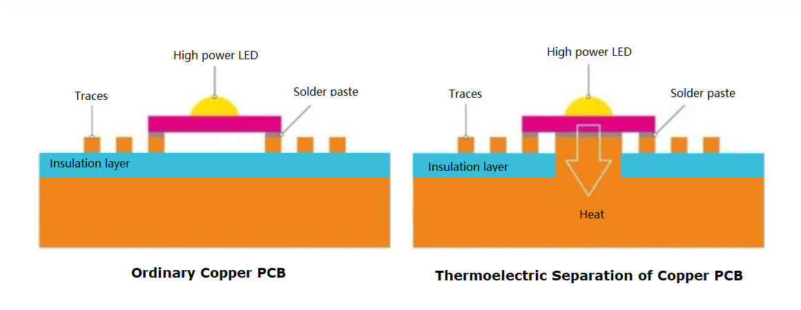
However, with the development of high-power electronic products and high-frequency PCBs, aluminum PCBs can no longer meet the requirements of heat dissipation and volume. Therefore, more and more products choose copper PCB, which has a thermal conductivity of up to 400W, 400 times that of aluminum PCB. But ordinary copper PCB also has a drawback, that is, its circuit layer and heat layer are on the same layer, which requires connecting the beads and the heat layer through an insulating thermal conductive material, which will reduce the thermal efficiency. To solve this problem, a more advanced copper PCB structure has emerged, called thermal-electric separation copper PCB or SinkPad PCB.

(Thermal_electric_separation_copper_pcb)

Introduction to Thermal-electric Separation Copper PCB

The feature of thermal-electric separation copper PCB is that its circuit layer and heat layer are on different layers so that the beads can directly contact the heat layer, achieving zero thermal resistance heat dissipation. This structure can greatly improve the luminous efficiency and lifespan of the beads, and reduce light decay and heating. Thermal-electric separation copper PCB is very suitable for single high-power beads, especially the COB package, which can make the lamp achieve better effects. In addition, thermal-electric separation copper PCB can also be made into different shapes and structures according to different design needs, such as copper protrusions, copper recesses, parallel heat dissipation, etc.

Below is the structure diagram of ordinary copper PCB and copper substrate bump thermoelectric separation as an example to give you a more intuitive understanding of the advantages of thermoelectric separation copper substrate processing technology.

(Diagram_structure_comprasion)

From the ordinary copper PCB diagram on the left, it can be seen that the heat dissipation needs to pass through the insulating and thermally conductive material (purple part in the picture), which is more convenient to process. However, after passing through the insulating and thermally conductive material, the thermal conductivity is not so good. This kind of suitable for low-power LED lights, which is enough.

If the heat dissipation requirements are very large on automotive LED lamp beads or high-frequency PCBs, both normal aluminum PCB and copper core PCB cannot meet the requirements. It is common to use thermoelectric separation of copper substrates. Because the circuit trace and thermal layer are on the different layers, the thermal layer part directly contacts the LED beads (as shown on the right side of the picture above) to achieve the best heat dissipation (zero thermal resistance) effect.

Besides, there are also many various surface treatment options for the thermal electric separation copper PCB, such as OSP, immersion gold, ENIG, immersion silver, silver plating, ENEPIG, etc. It can be carried out according to different needs, and the surface treatment layer and lifespan are reliable.

Who Can Make Thermal-electric Separation Copper PCB for You?

When you are considering to sample or order thermal-electric separation copper PCBs, it is recommended to choose Best Technology. Best team is a professional PCB manufacturer who specializes in PCB manufacturing for over 17 years of experience and provides excellent before and after-sales service. Now, Best Technology highly recommends thermal-electric separation copper PCB for you, and the price is very favorable right now. And we promise that we will make satisfactory thermal-electric separation copper PCB for you with the fastest speed and the highest quality. This is what we are proud of.

If you have any questions or comments about thermal-electric separation copper PCB or more information about our company, please feel free to contact us or e-mail us at sales@bestpcbs.com. We will serve you wholeheartedly.

You may also like

What Is Ceramic Metallization Technology? – Series 1
Saturday, October 7th, 2023

Due to the different surface structures of ceramic susbtrates and metal materials, welding/soldering often cannot wet the ceramic surface or form a strong bond with it. Therefore, the joining of ceramics and metals is a special process, which called as metallization.

What Ceramic Metallization Technology Is?

Ceramic metallization refers to the process of firmly attaching a thin layer of metal film to the surface of a ceramic material to achieve a bond between the ceramic and metal. There are various methods for ceramic metallization, commonly including molybdenum-manganese (Mo-Mn) method, directly copper plate (DPC), directly bonded copper (DBC), active metal brazed (AMB) method and more.

Which Ceramics Can Be Used Metallization Technology?

At present, there are four common ceramic substrates that always used for metallization, they are BeO, Al2O3, AlN and Si3O4. But different ceramic has different characteristics, so its metallization method also is different.

  • BeO Ceramic

The most common method for metallizing BeO ceramics is the Mo-Mn method. This involves applying a paste-like mixture of pure metal powders (Mo, Mn) and metal oxides to the ceramic surface, followed by high-temperature heating in a furnace to form a metal layer.

  • Al2O3 Ceramic

The primary metallization methods for Al2O3 ceramics are DBC and DPC. This method involves placing a treated copper foil on the surface of Al2O3 ceramics, introducing an inert gas with a certain oxygen content, and then heating. During heating, the copper surface undergoes oxidation, and when the temperature reaches the eutectic liquid phase region, a eutectic liquid phase is formed, wetting both Al2O3 ceramics and copper, achieving a tight bond. In a chemical sense, the adhesion used by DBC is stronger than DPC since it has thicker copper.

  • AlN Ceramic

Common methods for AlN ceramics include DBC and Active Metal Brazing (AMB). DBC is similar to the method used for Al2O3 ceramics but requires pre-oxidation treatment of AlN ceramics since AlN is a non-oxide ceramic. AMB involves connecting AlN ceramics and copper foils using active metal brazing materials, often Ag-Cu-Ti alloys.

  • Si3N4 Ceramic

Si3N4 ceramics cannot be directly metallized using the direct copper plating method because they do not generate an oxide layer on the surface like AlN ceramics. Si3N4 ceramics are typically connected to metals using the AMB method, where chemical reactions between Si3N4 and active metals (Ti, Cr, V) form continuous nitride layers at the interface.

What is the Metallization Temperature?

During the metallization process, the sinter temperature should be controlled strictly. Normally, it can be divided into four ranges:

  • Ultra-High Temperature (Above 1600°C):

This temperature range is reserved for specific applications where extreme heat resistance is required.

  • High Temperature (1450°C to 1600°C):

High temperatures are essential to ensure that the glass phase spreads and migrates effectively, enabling a strong bond. However, excessively high temperatures can lead to reduced metallization strength.

  • Mid-Temperature (1300°C to 1450°C):

This range is chosen to balance the need for effective metallization with the preservation of material properties.

  • Low Temperature (Below 1300°C):

Lower temperatures are used when the primary concern is avoiding thermal stress on the materials involved.

Proper high sintering temperature is necessary, otherwise, the glass phase will not spread and migrate. But if the temperature is too high, the metallization strength will be poor. So, choose a suitable temperature is important to make sure the metallization effective.

This is all the information about metallization technology, in our next blog, we will delve into what factors will affect the metallization. If you are interested in metallization or other technologies about ceramic circuit boards, please leave your message and keep your eyes in Best Technology website.

You may also like