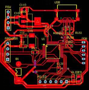
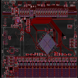
Electronics devices and parts are existing everywhere in this big data era, and more and more engineers trying to step in the electronics design and development. As a one-stop PCB and PCBA manufacturer in China, Best Technology would like to share some basic considerations and tips during the PCB designs. Hope this can help you.
Substrate Material
Substrate is the main composition of a circuit board and it mainly used for suppler and copper foil insulation. The commonly materials are FR4 and PI. FR4 is a widely acceptable international grade for fiberglass reinforced epoxy laminated, and it always used for making rigid PCB or rigid-flex PCB. FR4 substrate has good insulation and mechanical strength, so it can be widely used in various applications. However, PI has higher heat and chemistry resistance, more suitable for high temperature and chemical corrosion environment.
Circuit Layout
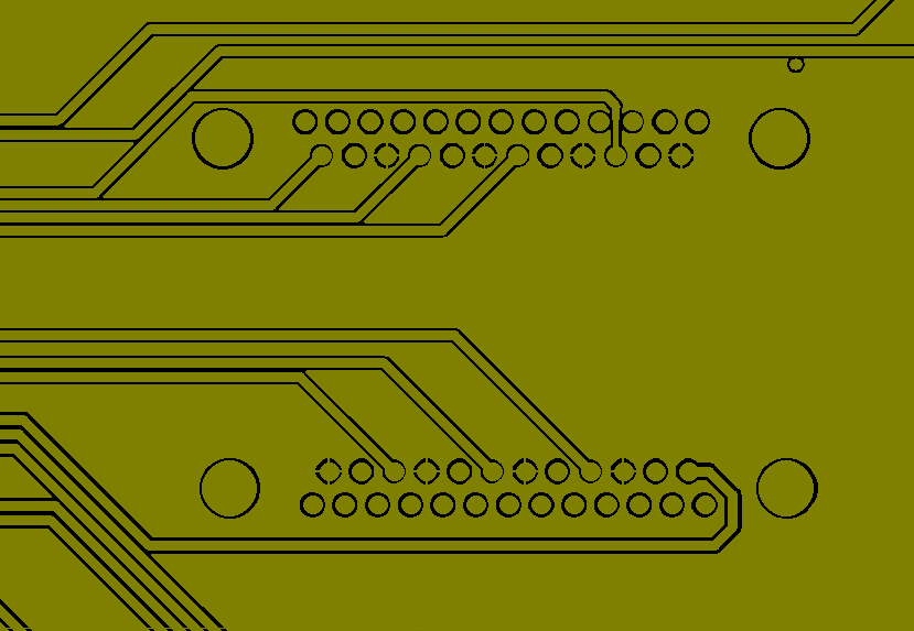
The layout design depends on the dimensions, performance and reliability of a circuit board, it is needed to follow your supplier’s standard to make sure the fast production time and high quality.
- Min line width
Please make sure your line width within your supplier’s manufacturing capability, that is to say, if it is less than the minimum line width will not able to be produced. The best way is if the design conditions available, the larger the line width, the better the factory production. Generally, the line width keeps around 10mil is the best. In another word, if your line width is less than normal standard, it would be difficult for you to find a suitable supplier.
- Min line spacing
Min line spacing means the distance between trace and trace. Normally, from the production aspect, the distance from line to pads should not less than min line spacing, and it would be better if it is larger, generally equal to or more than 10mil.
- The spacing between circuit to outline should be control in 20mil.
Plug-in Hole
The diameter of plug-in hole should be considered by the side of components, but it is necessary that it must greater than the component’s pins, it is recommended that greater at least 0.2mm. That is to say, if the pin of components is 0.6mm, then the plug-in holes should be greater than 0.8mm. Otherwise, the plug-in components would be probably difficult to insert into PCB because of the tolerance control during the manufacturing and assembly.
Min Hole Diameter
As we all know, the holes in PCB almost be used for mounting components, connect circuit and provide the electrical connection between layers. So how to design the hole also is crucial during the designing. Generally, the min hole diameter depends on the drill bitter that vendor used, always around 0.2-0.4mm. You can ask your supplier during the design evaluation.
Copper Thickness
Copper foil is a layer of metal foil on the PCB board that is used to conduct current. The thickness of copper foil is usually in oz (ounces), such as 1oz, 2oz, 3oz, etc. The thickness of the copper foil will affect the conductivity and heat dissipation performance of the PCB board.
Impendence Control
Impedance control is a key parameter in high-speed signal transmission and high-frequency circuit design. It involves board thickness, copper foil thickness, substrate dielectric constant, pad and line layout and other factors to improve the signal integrity and anti-interference ability of the PCB board.
The production process of PCBs is rather complex, involving a wide range of techniques from simple mechanical processing to sophisticated machining, so you should understand the design rules very clearly when you are trying to design a PCB board. Its applications are also diverse, from consumer electronics to industrial machinery, where PCBs are utilized.
Best Technology offers one-stop PCB solutions, we offer service from prototyping to large-scale production and assembly. With experienced engineers and service teams, we ensure successful fulfillment of your requirements. Just send us with your design files, and we will make the circuit board for you in a very short time.
Tags: design guide, pcb design


