
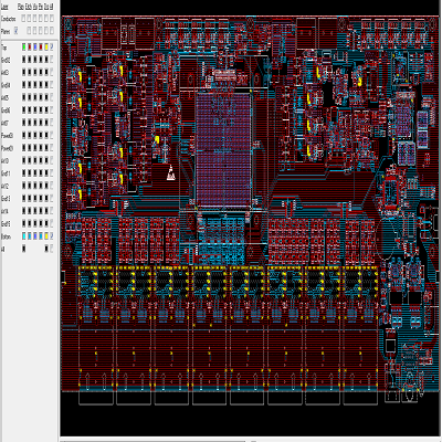
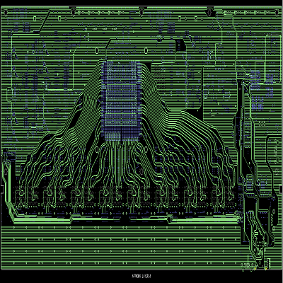
PCB design is one of an important process before the PCB manufacturing, it determines the overall performance of the whole product. We are an experienced PCB design and manufacturing vendor, with our professional technical team and advanced evaluated tools, we can make sure the PCB design one-time success. Today, we shared a example of fiber optical SFP modules design:
32X100G(QSFP28) large capacity convergence shunt
[1]: Marvell: 98CX8522
[2]: Single pair differential line, 25G optical network
[3]: 16 layers PCB
How to design a SFP optical module PCB?
SFP optical module interface PCB design depends on many aspects, including interface signal processing, timing control, power management and so on.
1. Determine the interface standard: SFP optical module interface standards, such as SFP, SFP+, QSFP and so on, you need to choose the appropriate interface standard according to the specific needs.
2. Choose the chip solution: According to the interface standard, choose the appropriate chip solution, usually including constant voltage source, amplifier, comparator, clock generator, EEPROM, etc.
3. Signal processing: For receiving and sending signals, filtering, amplification and comparison are required to ensure signal quality and stability.
4. Timing control: The timing and frequency of the clock signal need to be accurately controlled to ensure the correctness and stability of data transmission.
5. Power management: SFP optical module interface requires multiple power supplies, including Vcc, VCC-TX, VCC-RX, etc. Reasonable power management is required to ensure the stability and reliability of the power supply.
6. PCB design: According to the above requirements, PCB design is carried out, considering signal isolation, layering layout, status separation, signal integrity and other factors.
Feel freely to send message us if you are interested in PCB design.
You may also like


Tags: pcb design