
When designing high-speed PCBs, several critical factors must be considered to ensure optimal performance. These include signal integrity, impedance control, and minimizing electromagnetic interference (EMI). Below is an ultra high speed camera PCB solution made by Best Technology:
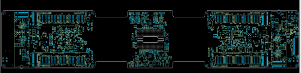
An ultra-high-speed camera rigid-flex circuit board
[1]: XCKU060 chip
[2]: 20A maximum current
[3]: Four DDR4 channels
[4]: 20 layers PCB
Camera PCB design considerations:
1. When the Camera adopts a connector: when the MIPI differential signal passes through the connector, the adjacent differential signal pairs must be isolated using GND pins; If it is not convenient to punch holes, the spacing between the difference pairs is at least 15mil.
2. If there is a reserved test point for the Camera connection seat, it should be close to the connection seat, and the Stub on the cable should be as short as possible.
3. Decoupling capacitors of AVDD/DOVDD/DVDD power supply need to be placed as close as possible to the Camera connection base.
4. The Camera layout needs to be far away from high-power radiation devices, such as GSM antennas.
5. CIF/MIPI and other signals, if there is a board to board connection through the connector, it is recommended that all signals be connected with a certain resistance value (between 2.2ohm and 10ohm, depending on the SI test), and reserve TVS devices.
Best Technology offers one-stop solutions for our values customers. And we provide free technical support for our customers. If you have similiar requirements, welcome to contact us at any time!


