
PCB design not only including the routing layout, component placement also is a key parameter. It involves understanding electrical parameters, signal integrity, and thermal management. This article will introduce several golden rules of how to optimize your component placement, whether you are a novice or a seasoned professional, it is helpful for you to manage your circuit board design greatly.
- Determine the power supply and grounding plane
In the early stage of PCB design, reasonable power supply and grounding layout is the key. The power supply and ground plane not only provide a stable power supply for the components, but also play a role in reducing electromagnetic interference (EMI). To begin the layout, the first thing is confirming the location of the power supply and ground area. Usually, the power is placed in a complete layer of the PCB, and the ground is in another layer, which can effectively reduce the power supply noise.
Make sure the power plane is close to the area where high power is needed, which can reduce the voltage drops along the supply path. The ground area should be as large and continuous as possible, this helps to provide a good return path and reduce interference from high-frequency signals.
- Differentiate layouts by function
When laying out components, dividing the circuit board into different functional areas can improve the efficiency and performance of the design. For example, you can separate power supply into signal processing area, power management area, and interface. This method helps to reduce the mutual interference between different circuits and improve the overall stability of the circuit.
Please noted that, high-frequency components should be close to connectors or key interfaces to shorten the signal path and reduce interference. Low-frequency components can be placed away from critical signal paths to optimize overall signal integrity.
- Keep short and direct trace
Shortening the length of signal lines is another important thing to optimize component layout. Make sure keep them short and direct as possible. Long distance signal routing may lead to signal attenuation and delay, which will affect the overall performance of the circuit. Placing the relevant components as close as possible. This not only reduces the length of the circuits, but also reduces the coupling and interference between the signals.
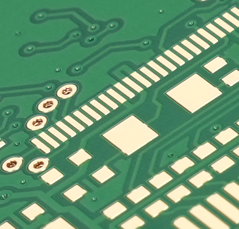
In addition, in the routing process, try to avoid right-angle (90 degrees) turns. Because the right angle will cause signal reflection, affecting the integrity of the signal. Try to use 45 degree turns or arc turns to reduce signal loss.
- Consider heat dissipation requirements
Heat management is an important consideration when placing high-power components. Place power components in the edge area of the PCB, such as power transistors and high-frequency converters. This facilitates the use of natural air flow for heat dissipation and convenient for the installation of external cooling devices.
In high-density designs, through-holes, vias and cooling copper blocks can be designed on the PCB, which can transfer heat to the inner layer or bottom of the PCB to help dissipate heat. In addition, maintain a reasonable distance between each component to promote air flow and heat dissipation.
- Optimize test points position
Consider placing test points in a convenient location for testing and debugging. Placing test points close to relevant components simplifies the debugging process and reduces test complexity. In particular, the placement of test points on the key signal path can facilitate the detection and verification of signal integrity and stability in the design stage.
For example, the discrete components required for OpAmp operational amplifiers can be placed close to the device, so that the bypass capacitors and resistors can work with them. This helps to optimize the wiring length mentioned as above, while also making testing and fault detection easier.
- Consider DFM & DFA factors
Optimizing component layout takes into account not only electrical performance, but also the actual requirements of manufacturing and assembly. For example, try to avoid placing components on both sides of the PCB to simplify the PCBA assembly process. The components are arranged neatly and spaced consistently, which helps the automated assembly equipment to operate efficiently and reduce assembly errors.
Properly using DFM (Design for Manufacturability) principles make production easier and more cost-effective. Ensure that your design can be fabricated with standard processes.
- Perform DRC as often as possible
Although it only takes a short time to run DRC (Design Rule Check) functionality on PCB software. But in some complex design environments, perform checks during the design process can save a lot of time, which is a good habit to keep. Every layout routing decision is critical, and running DRC can remind you of the most important layout at any time.
- Check production files before sending to manufacturer
While most of PCB manufacturers are happy to download it directly and verify it for you, it is best to export the Gerber file yourself and use the free software such as Gerberv to check that it is as expected to avoid misunderstandings. By verifying it yourself, you may even find some inadvertent errors and thus avoid the cost of completing the production according to the wrong parameters.
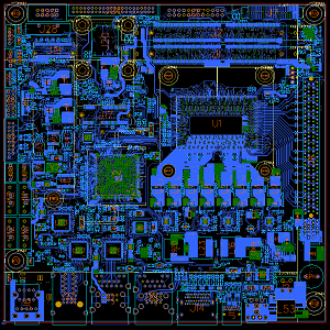
Successful PCB design cases – Best Technology
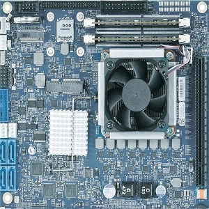
A: A mITX architecture industrial control main board
[1] Intel Xeon E3, Core™ i7/i5, Celeron G3900E processors
[2]:2x DDR4 SODIMM 2133 MHz (up to 32 GByte)
[3]:4x SATA Gen 3.0
[4]:1x PCIe x16 (Gen 3)
[5]:2x USB 3.0 (Internal) + 1x USB 3.0 (Client) + 2x USB 3.0 (Rear I/O) + 2x USB 2.0 (Rear I/O) +
2x USB 2.0 (Front Header) + 1x USB 2.0 (mPCIe)
Anyway, communicating with your manufacturer to understand their equipment and processes can optimize the design, reduce manufacturing problems, improve production efficiency and product quality.
You may also like


Tags: pcb design