Although semiconductor integration is increasing, many applications have ready-to-use systems on chip. And there are various powerful and out-of-the-box development boards are becoming more readily available, many use cases in electronics still require the use of custom PCBs. In one-time development, even an ordinary PCB can play a very important role. This article will introduce several golden rules of PCB design, and are widely applicable to various PCB design projects.
What are the golden rules of PCB design?
The golden rules of PCB design serve as the foundation for a robust layout. Remember below top 5 rules can help you in PCB designing.
- Optimize component placement
- Select correct crosstalk
- Make sure short and straight circuits
- Manage the distribution of power and ground circuit whenever possible.
- Avoid sharp angles in traces, opting for 45-degree turns instead.
Additionally, always perform Design Rule Checks (DRC) to catch potential issues before finalizing the layout. These checks help ensure compliance with manufacturing and performance standards.

What are the top 3 important steps in PCB design and layout process?
The PCB design and layout process has many important steps, but these three processes should be given priority.
1. Schematic design and component selection
Start by creating a detailed schematic diagram of your circuit board. As a designer, you can choose discrete components with high or low component values, but with the same performance. By consolidating within a smaller range of standard values, the bill of materials (BOM) can be simplified and potentially cost reduced.
Select suitable components based on the requirements of your design, considering factors like voltage, current, and signal frequency. A clear and precise schematic is essential. It helps avoid errors and streamlines the layout process, making it easier to place and route components effectively.
2. Component placement
Arrange components strategically on the board. Place critical components like microcontrollers and high-frequency ICs first, followed by supporting components. Consider heat dissipation and accessibility for debugging. If you have a range of PCB products based on preferred component values, it will also help you make the right inventory management decisions in the longer term.
3. Routing
Routing including connecting the components with traces. Prioritize routing for critical signals first, such as clock lines and high-speed data paths. Use the shortest possible paths and avoid crossing different signal types to reduce interference. After critical traces, route the power and ground nets, followed by less critical signals. Utilize multiple layers if needed to keep the layout clean and manageable.
What are the guidelines for PCB layout?
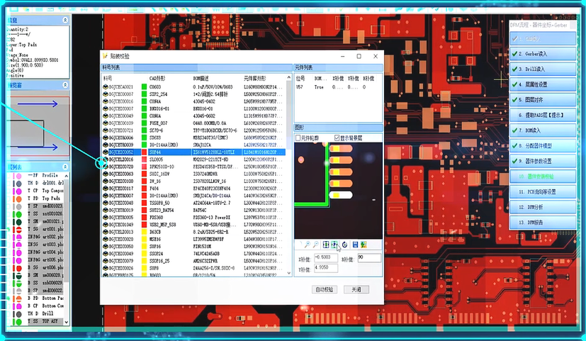
PCB layout guidelines can help designers achieve optimal component placement and ensure the board is easy to assemble. Here are some things to consider:
1. Trace width and spacing
Maintain appropriate trace width and spacing based on current carrying capacity and voltage levels. The IPC-2221A standard provides recommendations on PCB trace width and spacing. According to this standard, the trace width must be selected based on current-carrying capacity and permissible temperature rise. For instance, a 1mm wide trace with 1oz. copper (35μm) can carry approximately 2.5A with a 10°C temperature rise.
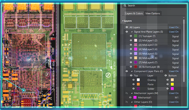
2. Layer stack-up
Design your PCB stack-up carefully. Multilayer designs are typically used in high-frequency applications to effectively separate power, ground, and signal layers, thereby reducing electromagnetic interference (EMI). Studies show that in a 4-layer or more stack-up, closely coupling the power and ground planes can significantly reduce EMI and improve signal integrity.
3. Thermal management
Consider thermal aspects in your layout. Place components that generate significant heat, such as power transistors, away from heat-sensitive components. Use thermal vias and heat sinks to manage heat dissipation effectively.
4. Via placement
Use vias strategically to connect different layers. Avoid placing too many vias close to high-frequency signal paths to prevent signal degradation. Use via stitching to enhance ground planes and reduce loop areas.
5. Power distribution
Using wide traces for power and ground planes is critical to minimizing resistance and inductance. For instance, IPC-2152 provides guidelines on power distribution and suggests using wide traces to handle higher currents and minimize voltage drops.
What are the considerations of PCB layout?
When designing a printed circuit board, you can consider these points:
1. Signal integrity
Maintain signal integrity by minimizing trace lengths and avoiding impedance mismatches. Use differential pairs for high-speed signals and keep them close together to reduce noise.
2. EMI/EMC
EMI and EMC are critical considerations. Use proper shielding and grounding techniques to mitigate interference and ensure compliance with regulatory standards.
3. Design for Manufacturability (DFM)
Ensure your layout is manufacturable by adhering to fabrication capabilities and tolerances. Simplify routing and avoid excessive component density to facilitate easier assembly and inspection.
4. Mechanical constraints
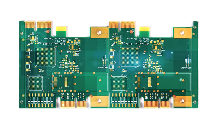
Consider the physical dimensions and mounting requirements of your PCB. Ensure that components and traces do not interfere with mechanical parts or enclosures.
5. Cost
Optimize your design for cost by reducing layer count where possible and minimizing the use of expensive materials or processes. Balance performance requirements with budget constraints.
At Best Technology, we offer expert design services to help you achieve your project goals with precision and excellence. Choose us for your next PCB project and experience the benefits of quality and innovation.
Tags: pcb design


