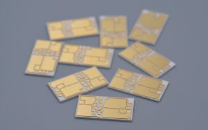
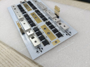
With the increasing demand of electronic devices working in high temperature environment, DPC (Direct-Plated Copper) ceramic PCB has been widely used as a heat dissipation material with strong high temperature stability and high thermal conductivity. This paper discusses the design and application of DPC ceramic substrate from the aspects of material, structure and technology.
Material Selection of DPC Ceramic PCB
It is very important to select ceramic substrate with good high temperature stability and high thermal conductivity. Commonly used ceramic materials are Al2O3, AlN, Si3N4 and so on. Taking Al2O3 as an example, its thermal conductivity is as high as 24~30W/(m·K), and the coefficient of thermal expansion is about 8.2×10^-6/℃, which is similar to the coefficient of thermal expansion of most chips. The ceramic layer on the surface of the substrate should be smooth and uniform, and have good adhesion, oxidation resistance, wear resistance and corrosion resistance.
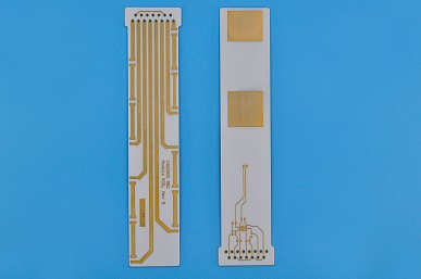
The heat dissipation performance of DPC ceramic substrate is one of the key factors affecting its work in high temperature environment. In order to test the heat dissipation performance of DPC ceramic substrate, thermocouple temperature measurement, infrared temperature measurement, thermal imager and other testing methods can be used. The experimental results show that the DPC ceramic substrate has good heat dissipation performance and can effectively heat dissipation and reduce the influence of temperature on electronic devices.
DPC Ceramic PCB Structure Design
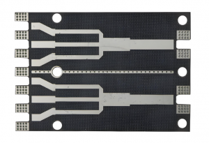
The structure design of DPC ceramic substrate includes the thickness of copper foil, the size of aperture, the layout of copper foil and the thickness of ceramic substrate. The choice of copper foil thickness should be determined according to heat dissipation requirements and chip power density and other parameters.
There are two layout methods of copper foil, one is fully plated surface; The other is local copper, that is, only the copper foil is laid in the area around the chip. The local copper laying method can reduce the copper foil area and reduce the cost, but the adhesion between the copper foil and the substrate needs to be higher. The thickness of the ceramic substrate also needs to be selected according to the specific application requirements.
PVD Process of DPC Ceramic PCB
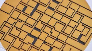
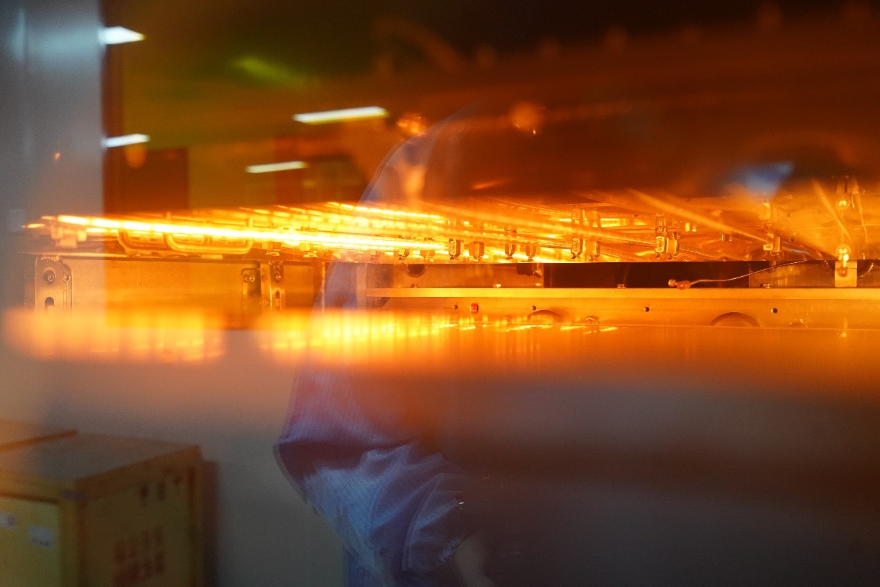
Direct Plating Copper (DPC) is a ceramic circuit processing technology developed on the basis of ceramic film processing. In this process, the copper metal composite layer is sputtered on the ceramic substrate by vacuum coating, and then the circuit is made by re-exposure, development, etching and film removal with the photoresistance of yellow light microshadow. Finally, the thickness of the circuit is increased by electroplating/electroless deposition, and the metallized circuit is made after the photoresistance is removed.
The process is the process of vaporizing metal materials (titanium and copper) into molecules and then forming a metal film on the surface of a ceramic substrate. The main process includes cleaning the surface of the substrate, heat treatment of the ceramic substrate, preparation of the target of metal materials, DPC of the target, measurement of film thickness and surface treatment. Among them, heat treatment can improve the thermal stability and adhesion of the ceramic substrate, and ensure that the covered copper foil will not peel off in high temperature environment.
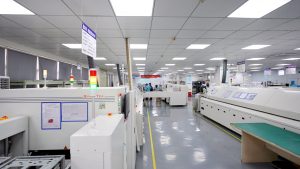
DPC ceramic substrate small size, precision structure, high reliability requirements, complex process flow, fine production process, belongs to technology-intensive industries, with high technical barriers. Its production process mainly involves drilling, magnetron sputtering, chemical copper deposition, copper plating, solder resistance printing, chemical silver/chemical gold deposition and other main processes
Application of DPC Ceramic PCB
a. VCSEL package
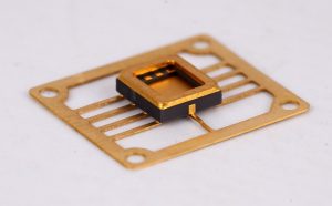
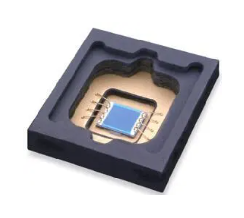
The power density of VCSEL is very high, and the DPC ceramic circuit board has a high thermal expansion coefficient matching with VCSEL, so as to solve the stress problem caused by the mismatch of thermal expansion between chip and substrate. The DPC ceramic circuit board makes the metal edge closely combined with the ceramic substrate, avoiding the additional paste process, coordination accuracy and other problems in the later assembly process, as well as the reliability problems caused by the aging of the glue. The ceramic circuit board of DPC film technology almost meets the packaging requirements of VCSEL.
b. IGBT package
The insulated gate bipolar transistor has become the mainstream of the development of power semiconductor devices due to its high input impedance, fast switching speed, low on-state current and high blocking voltage. Its applications are as small as frequency conversion air conditioning, silent refrigerator, washing machine, induction cooker, microwave oven and other household appliances, and as large as electric locomotive traction system. Due to the high output power and high heat output of IGBT, heat dissipation is the key for IGBT packaging. At present, the DPC ceramic substrate is mainly used for IGBT packaging, because the DPC ceramic substrate has the characteristics of large metal layer thickness, high bonding strength (good thermal impact) and so on.
c. LED package
Throughout the development of LED technology, the power density continues to improve, and the requirements for bracket heat dissipation are becoming higher and higher. DPC ceramic substrate has high insulation, high thermal conductivity and heat resistance, low expansion and other characteristics, especially the use of through hole interconnection technology, well meet the LED flip, eutectic, COB (chip on board), CSP (chip scale package), WLP (wafer package) packaging needs, suitable for medium and high power LED packaging.
In conclusion, the design and application of DPC copper-coated ceramic substrate need to consider many factors, and a lot of experiments and data analysis are required. The performance and reliability of DPC ceramic substrate at high temperature can be improved by selecting suitable materials and designing reasonable structure and process, and the high temperature application of microelectronic devices can be guaranteed.
The advent of DPC ceramic substrate products opens the development of heat dissipation application industry. Due to the heat dissipation characteristics of the ceramic substrate, it has the advantages of high heat dissipation, low thermal resistance, long life and voltage resistance. With the improvement of production technology and equipment, the rationalization of product prices is accelerated, and the application field of LED industry is expanded.
Tags: dpc ceramic pcb


