
With the gradual deepening of electronic technology in various application fields, the highly integrated circuit board has become an inevitable trend. Under this situation, the disadvantage of traditional circuit board FR-4 and CIM-3 in TC (thermal conductivity) has become a drawback to delay the development of electronic technology. Though the metal core PCBs are known for their good thermal management, they hard to meet the fast heat dissipation and miniaturization of the devices at the same time. This is why ceramic PCB stands out.
What is Ceramic PCB?
A ceramic PCB is a type of PCB made from ceramic materials, such as alumina (Al2O3), ALN (aluminum nitride), or Beryllium Oxide (BeO). These materials are prepared by using thermal conductive ceramic powder and organic adhesive under the condition of below 250℃. Ceramic powders are not easy to made, especially for aluminum nitride powder, this is one of reasons that why ALN ceramic PCB is more expensive.
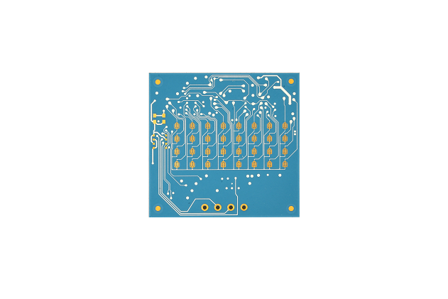
There are some different methods to make ceramic PCBs, commonly in the market are thick film, DBC, DPC and thin film technology. Different types of ceramic circuit boards have its unique characteristics. May you heard about HTCC, LTCC and AMB, they are also the ways to make ceramic PCBs, but there just a few manufacturers can make. Here is a HTCC ceramic PCB that we made.
Why Ceramic PCBs are popular used?
Different from the traditional FR-4 PCB (wave fiber), ceramic PCBs have good high-frequency properties, electrical properties that organic materials can’t achieved. It is a new generation of large-scale integrated circuits and power electronics module ideal packaging materials. The main advantages of ceramic circuit board including:
- Higher thermal conductivity
- More matched thermal expansion coefficient (CTE)
- Lower resistance
- Good weldability and can be used in high temperature
- Good insulation
- Lower high-frequency loss
- High density assembly available
- No organic ingredients, resistance to cosmic rays, high reliability in aerospace
- No oxide layer in copper layer, so it can be used for a long time in a reducing atmosphere
Who is the Best Ceramic PCB Manufacturer?
There are so many PCB manufacturers in the domestic and aboard, but reliable ceramic PCB vendors with good quality and reasonable price are very few. If you are looking for an experienced one, then keep the change. We’re the best option! Best Technology offers ceramic PCBs for our customers more than 100k every year, and we are high mixed from thick film ceramic PCB, DPC ceramic PCB, DBC/DCB ceramic PCB to AMB. Your PCBs need to use in automotives? Don’t worry, we gained IATF16949 and ISO13485 certifications, and all the manufacturing processes are strictly followed by ISO9001 quality control system. We welcome all the questions and inquiries from everyone.
Here is our ceramic PCB manufacturing capability for your reference.
| Ceramic PCB Manufacturing Capability | ||||
| No. | Item | General Parameter | Special Process | |
| 1 | Substrate | High insulation, chemical corrosion resistance, high-temperature resistance | Al2O3 | Glass, quartz, sapphire, 99% , 92% Al2O3 (black) |
| 2 | Excellent thermal conductivity, low thermal expansion coefficient, and high-temperature resistance | AIN | ||
| 3 | Insulation performance and high-temperature stability | ZTA | ||
| 4 | High strength, high hardness, high thermal conductivity, and low dielectric loss | Si3N4 | ||
| 5 | Conductor | Tungsten(LTCC/HTCC)、Au、Au&Pd、Au&Pb、Ag、Ag&Pd、Ag&Pb | ||
| 6 | Layer Count | DPC | Single – Double sided | |
| 7 | DBC | Single – Double sided | ||
| 8 | AMB | Single – Double sided | ||
| 9 | Thick film | Single – Double sided, 4L | ||
| 10 | LTCC | Single – Double sided, 4L, 6L | 6L – 14L | |
| 11 | HTCC | Single – Double sided, 4L, 6L | ||
| 12 | Copper Thickness | Inner layer | / | |
| 13 | Outer layer | Hoz-3oz (DPC), 3oz-12oz(DBC/AMB) | ||
| 14 | Dimension | Max. dimension | 130*180 | Larger dimension available (pass evaluation) |
| 15 | Min. dimension | 2*2 | Shipped in panel | |
| 16 | Substrate thickness | Al2O3/AIN 0.38. 0.635, 1.0mm, Si3N4 0.25、0.32mm | >1.5 | |
| 17 | Surface Treatment (thickness) | OSP | 0.2-0.5um | / |
| 18 | ENIG | 1-3u”(Au)120-320u”(Ni) | / | |
| 19 | Immersion silver | 6-12u” | / | |
| 20 | Immersion tin | ≥1um | / | |
| 21 | ENEPIG | Au 2u”, Pd 1U”, Ni 100u” | / | |
| 22 | Hard gold | 5-30u”(Au)、120-200u”(Ni) | / | |
| 23 | Drill | Min. PTH | 0.05MM | / |
| 24 | Min. NPTH | 0.05MM | / | |
| 25 | Max. aspect ratio (PTH PCB) | 5:1 | / | |
| 26 | NTPH tolerance | ±0.05 | / | |
| 27 | PTH tolerance | ±0.05 | / | |
| 28 | Line width/ Line spacing | Inner layer | Line width≥0.1mm; Line space≥0.1mm | 0.076/0.076mm |
| 29 | Outer layer | 1OZ; Line width≥0.12mm; Line space≥0.12mm | 0.1/0.1mm | |
| 30 | 2OZ;Line width≥0.2mm; Line space≥0.2mm | 0.15/0.15mm | ||
| 31 | 3OZ;Line width≥0.25mm; Line space≥0.25mm | 0.2/0.2mm | ||
| 32 | 4OZ;Line width≥0.35mm; Line space≥0.35mm | 0.3/0.3mm | ||
| 33 | 5OZ;Line width≥0.45mm; Line space≥0.45mm | 0.4/0.4mm | ||
| 34 | 6OZ;Line width≥0.55mm; Line space≥0.55mm | 0.5/0.5mm | ||
| 35 | Thick film; Line width≥0.1mm; Line space≥0.1mm | 0.076/0.076mm | ||
| 36 | Line width tolerance | ±20% | / | |
| 37 | Solder Mask (SM) /Silkscreen | Conductor | Glass glaze, medium, solder mask ink | / |
| 38 | SM color | White, black, green | Mixed color | |
| 39 | Silkscreen color | White, black | Mixed color | |
| 40 | Silkscreen height, width | Line width≥0.13mm; Height≥0.8mm | / | |
| 41 | SM thickness | ≥20um | / | |
You may also like


Tags: ceramic PCB, ceramic pcb board, ceramic pcb board manufacturer