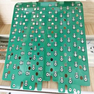
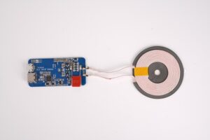
When it comes to PCB surface finishes, choosing the right one is essential for the longevity and performance of your circuit board. Among the many options available, two of the most popular are Hot Air Solder Leveling (HASL) and Electroless Nickel Immersion Gold (ENIG). These two methods offer distinct advantages depending on the application, and understanding their differences can help you select the best finish for your project.
What Does HASL Stand For?
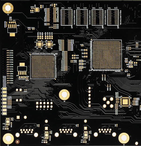
HASL stands for Hot Air Solder Leveling. It is a surface finish process used in PCB manufacturing. The term describes the method where solder is applied to the copper pads on a PCB and then leveled using hot air to ensure even coating. HASL is widely used because of its simplicity and effectiveness in providing a reliable solderable surface.
What Is HASL in PCB?
In PCB manufacturing, HASL is a surface finish applied to the exposed copper pads to protect them from oxidation and to provide a good surface for soldering components. The HASL process involves dipping the PCB into molten solder, typically composed of a lead-free alloy, and then using hot air to remove excess solder, ensuring a smooth and even layer. This finish is particularly valued for its excellent solderability and cost-effectiveness.
Characteristics of Hot Air Solder Leveling
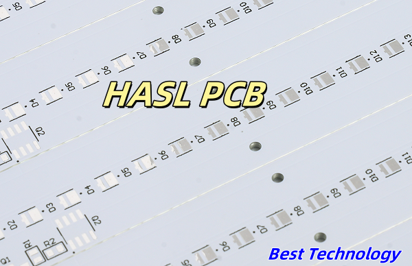
Hot Air Solder Leveling is a widely used surface finish in PCB manufacturing due to its unique set of characteristics that make it suitable for various applications. Below are the key attributes that define HASL:
1. HASL provides one of the most solderable surfaces available for PCB assembly. The molten solder applied during the HASL process creates a coating that is highly receptive to soldering, making it easy to attach components.
2. Compared to other surface finishes like ENIG or OSP, HASL is generally more affordable.
3. The solder coating provided by HASL serves as a protective layer for the copper pads on the PCB. This layer helps prevent oxidation and corrosion.
4. Variability in coating thickness. The hot air leveling process can result in uneven distribution of solder, leading to variations in thickness across the PCB. While this might be a drawback for designs requiring fine-pitch components or precise tolerances, it is often acceptable in less demanding applications where slight variations are not critical.
5. Thermal resistance. The solder layer provided by HASL can withstand multiple thermal cycles during the PCB assembly process, such as during solder reflow.
6. The HASL process creates a strong bond between the solder and the underlying copper pads.
What Is the HASL Method?
The HASL coating process is a critical step in PCB manufacturing, designed to protect the exposed copper pads and good solderability during the assembly of electronic components. The process is under several steps, each carefully controlled to achieve a uniform and reliable coating. Here’s a detailed look at how HASL is applied to a PCB:
1. Pre-Cleaning the PCB
The HASL process begins with thoroughly cleaning the PCB to remove any contaminants such as oxidation, oils, or residues from previous manufacturing steps. This is typically done using a combination of chemical cleaning agents and mechanical scrubbing.
2. Flux Application
After cleaning, a layer of flux is applied to the PCB. Flux is a chemical agent that serves multiple purposes: it removes any remaining oxidation from the copper pads, improves the wetting of the solder, and helps the solder adhere more effectively to the copper. The type of flux used can vary, but it must be compatible with the solder alloy to ensure a reliable coating.
3. Solder Bath Dipping
The PCB is then dipped into a bath of molten solder. For lead-free HASL, the solder typically consists of a tin-silver-copper (SAC) alloy, which is heated to a temperature between 240°C and 260°C (464°F to 500°F). The molten solder covers the entire surface of the PCB, including the copper pads and through-holes, forming a protective layer.
4. Hot Air Leveling
Once the PCB is removed from the solder bath, it immediately undergoes the leveling process. The board is passed through a pair of hot air knives positioned on either side. These knives blow high-pressure, heated air across the surface of the PCB, removing any excess solder and ensuring a uniform layer remains on the pads.
5. Cooling
After leveling, the PCB is cooled to solidify the solder coating. This cooling is typically done using an air or water-based cooling system, depending on the specific requirements of the manufacturing process. Rapid cooling can sometimes introduce stresses into the solder layer, so the cooling rate must be carefully controlled to avoid defects like cracking or warping.
6. Post-Process Cleaning
In some cases, the PCB may undergo a final cleaning step to remove any flux residues or other contaminants that might remain after the HASL process. And then testing and inspection.
What Is the Difference Between HASL and ENIG Finish?
While both HASL and ENIG are popular PCB surface finishes, they differ significantly in their composition, application, and performance:
| Characteristic | HASL | ENIG |
| Cost | Lower cost, suitable for budget-sensitive projects | Higher cost, but justifiable for high-reliability needs |
| Solderability | Excellent, but may vary with coating thickness | Consistent, even for fine-pitch components |
| Durability | Reasonable, but less effective in harsh environments | Superior, with excellent corrosion resistance |
| Thermal Performance | Good, but uneven surface might cause issues | Excellent, with consistent performance in high-heat scenarios |
| Best Suited For | General-purpose electronics, consumer products | High-reliability applications, aerospace, medical, and high-density PCBs |
| Surface Flatness | May have uneven surface, less ideal for fine-pitch components | Extremely flat surface, ideal for precise component placement |
| Environmental Impact | Lead-free HASL is environmentally safer, but traditional HASL uses lead which is harmful | Environmentally friendly, as it doesn’t use lead or other harmful materials |
| Shelf Life | Shorter shelf life due to potential oxidation over time | Longer shelf life due to gold’s resistance to oxidation |
| Reworkability | Easier to rework due to the nature of solder | More challenging to rework due to hard nickel layer |
HAL vs. HASL
HAL (Hot Air Leveling) and HASL (Hot Air Solder Leveling) are terms often used interchangeably, but they can refer to slightly different processes. HAL is a broader term that encompasses any method of leveling solder using hot air. In contrast, HASL specifically refers to using solder to coat the PCB’s surface. Essentially, all HASL processes are HAL, but not all HAL processes are HASL.
What Is the Composition of HASL?
At present, the solder of lead-free solder alloy hot air leveling is mainly Sn-Cu-Ni+Ge (germanium) or Sn-Cu-Ni+Co (cobalt). The components of Sn-Cu-Ni+Ge (Germanium) in the OPA2544T are Sn, 0.7% Cu, 0.05% Ni and Ge with a nominal content of 65×10-6. Germanium can not only prevent the growth of oxides, but also prevent the solder joints on the PCB pad coating surface from yellowing and tarnishing during the HASL process and subsequent reflow welding and wave soldering processes. In addition, germanium can also inhibit the formation of slag in lead-free wave soldering.
The biggest problem in the lead-free HASL process is the problem of sinking copper in the tin tank during the use of the equipment.
The typical operating temperature range of the HASL process is 265 to 275 ° C, and this temperature range can be used for almost all actual manufactured laminates. At this temperature, even CEM1, there is no problem of delamination and degradation. However, the actual process temperature increases with the increase of copper composition in the tin tank. When the copper composition is 0.3% higher than the optimal value of 1.2%, then the welding temperature must be increased to 285 ° C, which is not the laminate can withstand. Although a copper-free solder alloy can be added to reduce the copper content in the tin tank, it is difficult to control the proportion.
The so-called “freeze-drying” method can also be used. When the tin lead eutectic solder (63Sn-37Pb) temperature drops to about 190℃, the melting tin copper intermetallic compound (Cri6Sn5) will be “freeze-dried”. In high-density lead solders, Cu6Sn5 floats on the surface of the molten solder and can be skimmed out using a slotted spoon. However, in lead-free solder, Ct16SIl5 is denser than lead-free solder, and CLJ6Sn5 will settle to the bottom of the tin tank. There is a mechanism to reduce the temperature to about 235 ° C (about 8 ° C higher than the melting point temperature), the tin tank shut down for at least two hours, preferably all night, at this time, most of the alloy is still in a molten state, you can design special tools, from the bottom of the tin tank out of the precipitation of Cr16Sn5, but it is still very difficult.
What Is the Minimum Pitch for HASL?
The minimum pitch for HASL refers to the smallest distance between two adjacent pads that can be reliably soldered using the HASL process. Due to the nature of the hot air leveling process, which can create uneven surfaces, HASL is generally not recommended for very fine-pitch components. The minimum pitch is typically around 0.65mm, but it can vary depending on the specific requirements and the quality of the HASL process used.
Does HASL Oxidize?
One of the main concerns with any PCB finish is oxidation, which can affect solderability and reliability. While HASL provides a protective solder layer that helps prevent oxidation, it is not entirely immune. Over time, especially in harsh environments, the solder can oxidize, leading to potential issues during assembly. However, proper storage and handling can minimize this risk, making HASL a reliable choice for many applications.
How Thick Is the HASL Coating?
The thickness of the HASL coating can vary depending on the process parameters and the type of solder used. Typically, the thickness ranges from 1 to 25 microns. This variability can be a drawback for applications requiring precise and consistent thickness, especially for fine-pitch components. However, for many general-purpose applications, the thickness provided by HASL is more than sufficient.
What Is the Black Pad Syndrome?
Black pad syndrome is a phenomenon associated with the ENIG finish, not HASL. It occurs when there is an issue with the nickel layer during the ENIG process, leading to poor solder joints and potential failures. The term “black pad” refers to the appearance of the affected nickel layer, which turns black due to oxidation and contamination. While this issue is unrelated to HASL, it’s important to note that HASL does not suffer from black pad syndrome, making it a more straightforward and reliable finish in this regard.
When choosing between lead-free HASL and ENIG surface finishes for your PCB, it’s important to consider the specific needs of your project. For reliable and high-quality PCB manufacturer, consider working with Best Technology, a leader in the field. With our expertise and advanced technology, we ensure that your PCBs meet the highest standards of quality and performance. Whether you choose HASL or ENIG, we have the experience and capability to deliver the best results for your project.


