
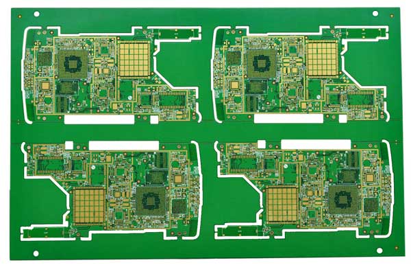
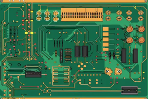
What is hdi pcb?
HDI stands for High Density Interconnect, which refers to high-density interconnect technology. HDI circuit board is a high-end printed circuit board with very high circuit density and complexity, which can achieve high-speed signal transmission and reliability design. The main features of HDI circuit board are multi-layer circuit, thin plate, small aperture, dense wiring and fine circuit. It is widely used in mobile phones, computers, network communications, automotive electronics and other fields. Bestpcb is a professional HDI manufacturer with 18 years of HDI manufacturing experience.
What are the advantages of hdi pcb
- Higher line density: HDI PCB can support more circuit tracks, arrange more electronic components in a limited space, and achieve high-density interconnection.
- Smaller device spacing: The micro-hole technology of HDI PCB allows smaller spacing between components, which is suitable for compact design.
- Improve signal integrity: The advanced stacking layer structure is adopted to provide better signal transmission quality and reduce signal interference.
- Improve reliability: The manufacturing process of HDI PCB improves the mechanical strength of the board, making it more durable and suitable for demanding application environments.
- Improve circuit integration: More line connections and component arrangements are achieved in a limited circuit board space to meet the needs of modern products that are thin and compact.
- Enhance signal transmission efficiency: The use of advanced wires and connection methods can increase the operating speed of electronic devices and reduce energy consumption.
- Support more complex system design: High-density connection capabilities provide support for complex system design and give full play to the performance of electronic devices.
- Promote innovation in the electronics industry: The application of HDI technology has promoted the innovation and development of the electronics industry, making electronic equipment more intelligent and efficient.
- Smaller size: It can complete a large number of circuit connections in a smaller space, meeting the needs of electronic products for lightness and portability.
- Higher signal transmission speed: The high-density line design allows signals to be transmitted quickly in a short time, improving the system operation speed and response speed.
Why does HDI PCB need via filling and plating?
Via filling plating plays a vital role in HDI PCB manufacturing, with the main purpose of improving electrical performance, connection reliability, operating frequency, and avoiding electromagnetic interference. This technology fills the blind holes of HDI PCB with conductive materials through the electroplating process to form a conductive path, which improves the performance and reliability of electronic equipment.
- Improve electrical performance: Via filling plating can improve the electrical performance of HDI PCB, especially in high-frequency circuit board design, which is crucial for improving connection reliability, operating frequency and avoiding electromagnetic interference.
- Via plugging and electrical interconnection in one step: Via filling plating technology combines via plugging and electrical interconnection, avoiding the defects caused by resin via filling, and also avoiding the CTE difference caused by other materials via filling.
- Improve efficiency: Compared with resin via filling or other materials via filling, via filling plating has a simpler process and higher efficiency.
- Process flow and technical challenges of via filling plating
- Process flow: including steps such as tank preparation, setting of electroplating process control parameters, and analysis of potion addition.
- Technical challenges: including positioning accuracy issues and electroplating quality issues, which need to be solved by strictly controlling parameters such as electroplating time and current density.
Application scenarios of hole filling electroplating
First-order HDI: Suitable for electronic devices with less complex circuits.
Second-order and above blind hole electroplating copper filling: Suitable for more complex electronic devices, such as mobile phones, laptops, etc.
Comparison between hole filling electroplating and full-board electroplating
Full-board electroplating: Although it can provide a uniform surface copper thickness distribution, it may encounter the problem of residual dry film on the board surface or in the hole during pre-treatment, resulting in some areas unable to be plated with copper. In addition, the etching process after full-board electroplating may cause quality defects such as side etching and fine lines.
Hole filling electroplating: Compared with full-board electroplating, hole filling electroplating is more accurate in filling blind holes, avoiding the problems that may be encountered in full-board electroplating, while simplifying the process and improving efficiency.
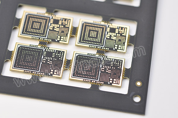
Materials of HDI PCB
The materials of HDI PCB mainly include coated copper foil (RCC), prepreg, copper foil, etc.
Resin-coated copper foil (RCC): This is a material that coats a special resin film layer on electroplated copper foil, used for HDI insulation layer. The characteristics of RCC include no glass dielectric layer, easy laser and plasma micro-hole forming, extremely high peel strength and good toughness, suitable for micro-narrow line etching. Laser drilling is performed on RCC, and the aperture shape formed is an inverted trapezoid, and the general aperture size is 0.076-0.10 mm. The use of RCC makes HDI PCB more widely used in small portable products, such as mobile phones, digital cameras, laptops, etc.
Prepreg and copper foil: These are basic materials in HDI PCB manufacturing, there are no special requirements, and they are suitable for different types of HDI PCB structures. The inner layer circuits are generally 1 ounce copper thick, while the outer layer circuits are plated with half an ounce of base copper to 1 ounce of finished copper thickness. The thickness of the board is usually thinner to meet the miniaturization requirements of HDI PCB.
Other materials: In addition to the main materials mentioned above, the manufacture of HDI PCBs may also involve other materials, such as FR4, PI (polyimide), BT, etc. These materials are selected according to specific application requirements. For example, FR4 has good electrical and mechanical properties and is suitable for most general applications; PI has higher heat resistance and chemical corrosion resistance, and is suitable for high temperature, high humidity and strong acid and alkali environments, but it is more expensive and difficult to process; BT combines good electrical properties, mechanical properties and thermal stability, and is suitable for application scenarios that require higher heat resistance.
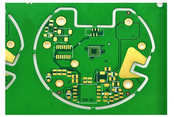
Classification of HDI circuit boards
HDI circuit boards are mainly divided into first-order, second-order, third-order, high-order (including fourth-order and above) and Anylayer HDI.
- First-order HDI circuit boards mainly include single-sided or double-sided micro-hole processes, and the circuit layer has only one layer. This type of HDI circuit board is suitable for applications with high requirements on cost and space, such as consumer electronics.
- Second-order HDI circuit boards contain two circuit layers, which are more complex but also more powerful than first-order HDI circuit boards. They can handle higher signal frequencies and are suitable for applications that require high performance, such as high-end communication equipment and computer hardware.
- Third-order HDI circuit boards contain three circuit layers. They are the most complex type at present. They can handle the highest signal frequency and the maximum data transmission rate. They are usually used in applications that require the highest performance, such as aerospace and military equipment.
- High-order HDI (including fourth-order and above) The applications of third-order or fourth-order HDI in electronic terminal products are more, while those above fourth-order are mostly converted to Anylayer structure.
- Anylayer HDI refers to HDI of any order/any layer. Compared with PCB boards with traditional lamination processes, HDI can reduce costs to a lower level when the stacking density exceeds eight layers. It also has higher electrical performance and signal accuracy, and significantly improves the performance of electromagnetic waves and radio frequency interference, electrostatic discharge and heat conduction in interconnection and relay transmission.
HDI PCB Process Flow
The process flow standards of HDI PCB mainly involve the application and processing technology of high-density interconnection technology (High Density Interconnection Technology, HDI for short), including first-order, second-order and third-order processes. Specifically, the HDI PCB process flow includes the following key steps and characteristics:
First-order process (1+N+1): This is a basic high-density interconnection technology that manufactures multi-layer boards through build-up and micro-blind via technology.
Second-order process (2+N+2): Further development on the basic technology, adding more layers and complexity.
Third-order process (3+N+3): Represents the highest stage of HDI technology, with extremely high layers and interconnection density
Differences between HDI PCB and ordinary PCBs
- Differences in circuit design:
HDI PCB adopts a more sophisticated circuit design, with smaller line width and spacing, and smaller aperture, which can integrate more electronic components and realize more complex circuit functions.
The blind, buried and stacked hole designs of HDI PCB greatly improve the utilization rate and signal transmission performance of the circuit board. - Differences in manufacturing process:
The manufacturing process of HDI PCB is more complicated, requiring high-precision processes such as laser drilling technology, hole filling electroplating technology and photolithography technology.
The manufacturing cost of HDI PCB is relatively high, but the performance and reliability are also higher. - Differences in application:
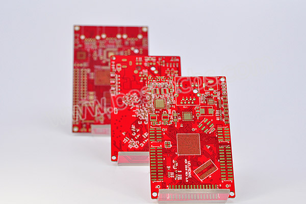
Due to its high density and high performance, HDI PCB is widely used in high-end electronic products, such as smartphones, tablets, high-end communication equipment, etc.
Ordinary PCB is mainly used in low-end electronic products and general electronic equipment. - Characteristics and application scenarios of HDI PCB:
HDI PCB has high-density wiring, multi-layer structure, high-precision manufacturing process and excellent electrical performance, which can meet the extremely high requirements of high-end electronic products for size, weight, performance and reliability.
HDI PCB is widely used in smart phones, tablet computers, high-end communication equipment and other fields, promoting the continuous development and upgrading of electronic products.
Application of HDI PCB
HDI PCB (High Density Interconnection Printed Circuit Board) is widely used in multiple industries, including medical equipment, mobile phones, laptops, automotive electronics, computer industry, and future 5G technology fields
- Medical equipment: The application of HDI PCB in medical equipment, such as sphygmomanometers and ultrasonic imaging systems, achieves accurate measurement of blood pressure and high-definition imaging of the internal structure of the body, providing patients with timely and accurate diagnosis and treatment information.
- Mobile phone industry: With the increasingly miniaturized design of mobile phones, HDI PCB is widely used in transceiver modules, motherboards, SIM card interfaces, fingerprint recognition modules and other parts of mobile phones due to its high density, high quality and high reliability.
- Computer industry: In the computer industry, the application of HDI PCB improves the performance of computers, especially in the fields of high-speed algorithms and multimedia applications, and adapts to the miniaturization trend of computer equipment2.
- Automotive electronics: HDI PCB has broad application prospects in the field of automotive electronics. In addition to the dominant mobile phone market, it also involves multiple fields such as automobiles, modules and artificial intelligence, demonstrating its key role in complex electronic systems.
- Future development trends: With the advent of 5G technology, the demand for HDI PCB will continue to increase, requiring higher speeds and frequencies while adapting to smaller and thinner device designs. Research new micro HDI PCB boards to adapt to future development trends.
You may also like


Tags: HDI circuit boards, HDI PCB, PCB