

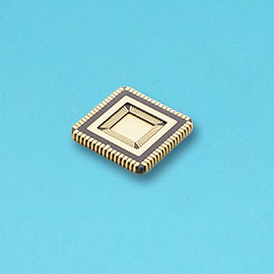
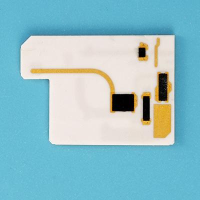
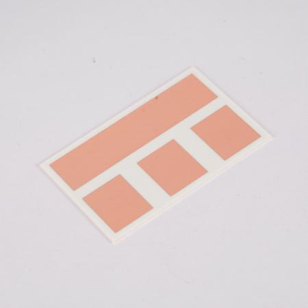
Ceramic PCB is composed of ceramic substrate, connecting layer and circuit layer. With the development of electronic industry, the types of ceramic PCB have become various. Since ceramic materials were used as PCB substrate, many methods for manufacturing circuit layer on ceramic substrate have been developed, among which several common ceramic circuit boards are HTCC (high temperature co-firing), LTCC (low temperature co-firing), DBC (direct copper cladding) and DPC (direct copper plating). Each type of ceramic circuit board has different usage scenarios, and also corresponds to different manufacturing processes.
How is the ceramic pcb made by HTCC process?
First of all, the starting material of HTCC (high temperature co-fired ceramics) process is ceramic powder (such as Al2O3 or AlN), and these materials need to be mixed with organic binder to form paste ceramic slurry. Then, the ceramic slurry is scraped into a sheet by using a scraper, and a green embryo is formed through a drying process. After the green embryo is formed, through holes are drilled according to the circuit layer design, and then the wiring and hole filling are carried out by screen printing metal paste. Finally, the germ layers are stacked and sintered in a high temperature furnace (about 1600 C).
Specifically, the HTCC process flow includes the following key steps:
Casting molding method: the ceramic slurry is scraped into a thin strip with uniform thickness, and dried by blowing filtered hot air opposite to the moving direction of the conveyor belt to form a green sheet.
Punching: Through mechanical drilling, mechanical punching or laser drilling, through holes are punched in the green blank. The size, position and accuracy of these holes directly affect the on-off and wiring density in the substrate.
Through-hole filling: the filling slurry is extruded into the through-hole of the green porcelain by mask printing method to complete the metallization process of the green porcelain.
Lamination, slicing and co-firing: the printed germ layers are laminated, then sliced and finally co-fired at high temperature.
After the completion of this series of steps, a high-temperature co-fired ceramic (HTCC) substrate is obtained, which has excellent electrical and mechanical properties and is widely used in the manufacture of electronic products requiring high performance.
How is the ceramic pcb made by LTCC process?
The first step is to prepare raw materials. The raw materials of LTCC are mainly composed of ceramic powder and organic additives. Ceramic powders, such as alumina and zirconia, are used to improve the insulation and mechanical strength of ceramic materials. Organic additives are used to increase viscosity and improve plasticity, which is convenient for the subsequent molding process.
Then there is circuit printing, the purpose of which is to print circuit patterns on ceramic substrates, usually using shielding printing technology. Firstly, the ceramic substrate is cleaned and coated with conductive metal ink. Then, the circuit pattern is transferred to the substrate by stamping with a printing die. Then, through the baking process, the conductive ink is solidified on the substrate to form a conductive circuit.
The third step is a sintering process, in which ceramic materials are chemically reacted at high temperature to combine their particles to form a compact ceramic body. In the process of sintering, the control of temperature gradient and atmosphere is very important to reduce the stress of materials and prevent them from oxidation.
In the final step of finished product inspection and subsequent treatment, the sintered ceramic substrate needs to be inspected first, including appearance quality inspection, size measurement, electrical performance test and other items. Qualified products can be subjected to subsequent electronic component packaging processes, such as welding, film covering, gas packaging, etc., to realize the protection and connection of electronic components.
To sum up, the manufacturing process of ceramic PCB by LTCC process involves many steps, such as precise material selection, processing, circuit printing, sintering, finished product inspection and subsequent treatment, to ensure the quality and performance of the final product.
How is the ceramic pcb made by DBC process?
The first step is the preparation of raw materials. First, it is necessary to select suitable ceramic substrate materials. Common materials include alumina (Al2O3) and aluminum nitride (AlN), which have high insulation, high thermal conductivity and good mechanical strength. The surface of the substrate should be cleaned and treated first to ensure the bonding with the subsequent copper foil.
Then the bonding between copper foil and ceramic substrate is the core step of DBC manufacturing process. At a certain temperature and pressure, the copper foil is closely attached to the ceramic substrate to form a firm bonding interface. It is necessary to control the parameters such as temperature, pressure and time in the bonding process to ensure the bonding quality and performance.
Secondly, after the bonding is completed, the copper foil needs to be etched to form the required circuit pattern. Chemical etching or laser etching can be used in the etching process. By precisely controlling the etching depth and width, high-precision and high-resolution circuit patterns can be obtained.
Finally, the DBC structure is cleaned, dried and tested. The purpose of this is to remove residues and improve the reliability and stability of products.
Through the above steps, high-performance DBC ceramic substrates can be prepared, which are widely used in the packaging of intelligent power modules and electric vehicle power modules.
How is the ceramic pcb made by DPC process?
Firstly, the ceramic substrate is pretreated and cleaned to ensure the cleanliness of the substrate surface and prepare for the subsequent deposition and copper plating process.
Then the key step is to deposit a Ti/Cu layer on the surface of the substrate as a seed layer by vacuum sputtering technology. This step is the most important in DPC process.
Followed by photolithography, development and etching processes, the circuit is completed.
Finally, the thickness of the circuit is increased by electroplating or electroless plating to enhance the conductivity and durability of the circuit. After the metallized circuit is manufactured, the photoresist is removed, and finally the substrate is manufactured.
The manufacturing process of ceramic PCB by DPC process involves vacuum sputtering, photolithography, development, etching and electroplating, which makes the ceramic PCB by DPC process have good conductivity and durability, and is suitable for various electronic application scenarios.
With the increasing use of ceramic PCB, in order to adapt to some application fields, many different process technologies have emerged, and each process technology has its own unique technology. For example, HTCC process needs to be sintered at high temperature to achieve its goal. According to the different environment used and the production cost, the appropriate ceramic PCB production technology is selected. BEST Technology has rich experience in manufacturing ceramic circuit boards. For different kinds of ceramic PCBs, there are different production lines and professionals. If you choose the right manufacturer, you will get the best quality ceramic circuit boards.