
When designing a PCB board, careful attention to stack-up and impedance control is essential for achieving optimal signal integrity and performance. The PCB stack-up refers to the arrangement of copper and insulating layers that make up the board. Impedance control, on the other hand, involves maintaining consistent electrical characteristics within signal traces, especially in high-speed circuits. This post provide a detailed guideline of PCB stack-up and impedance control for designers.
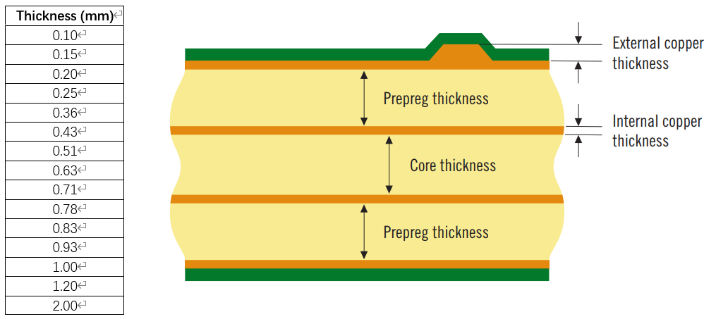
PCB Stack-up Parameter
Internal Copper Thickness After Processing
| Base Foil | Min. After Processing |
| 18um (1/2oz) | 11.4um |
| 35um (1oz) | 24.9um |
| 70um (2oz) | 55.7um |
| 105um (3oz) | 86.6um |
| 140um (4oz) | 117.5um |
External Copper Thickness After Plating
| Base Foil | Min. Class 2 | Min. Class 3 |
| 12um (3/8oz) | 29.3um | 34.3um |
| 18um (1/2oz) | 33.4um | 38.4um |
| 35um (1oz) | 47.9um | 52.9um |
| 70um (2oz) | 78.7um | 83.7um |
| 105um (3oz) | 108.6um | 113.6um |
| 140um (4oz) | 139.5um | 144.5um |
Common Prepreg (PP) Properties
| Type | Thickness (mm) | Resin (%) |
| 106 | 0.05 | 65 |
| 1080 | 0.075 | 65 |
| 2116 | 0.12 | 55 |
| 7628 | 0.2 | 46 |
Common Material List
| Medium Tg | Shengyi S1000-H |
| ITEQ IT-158 | |
| Elite EMC-825 | |
| High Tg | Shengyi S1000-2M |
| ITEQ IT-180A | |
| Elite EMS-827 |
Common Core Thickness
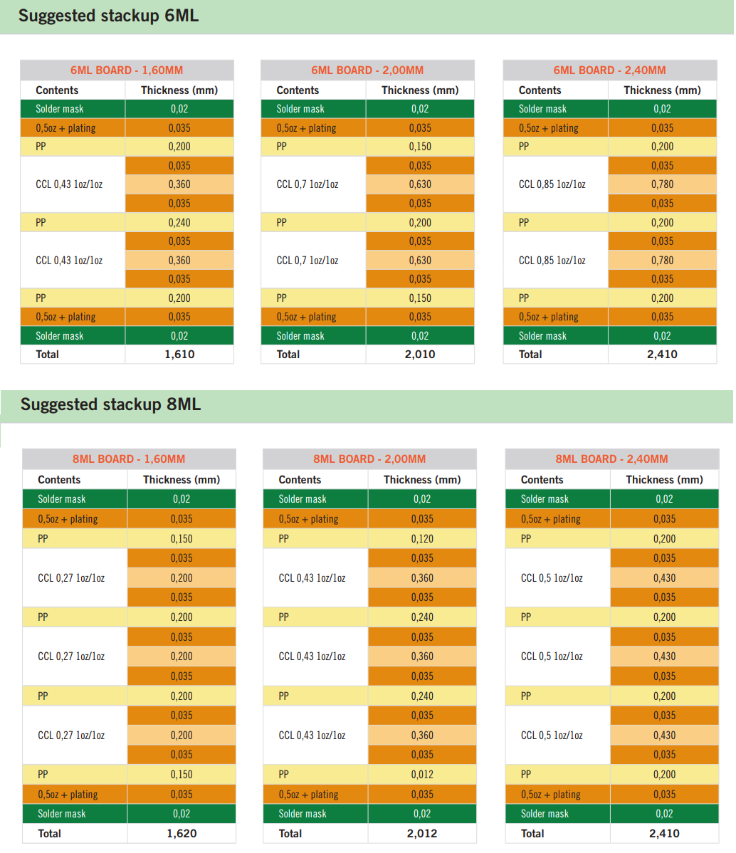
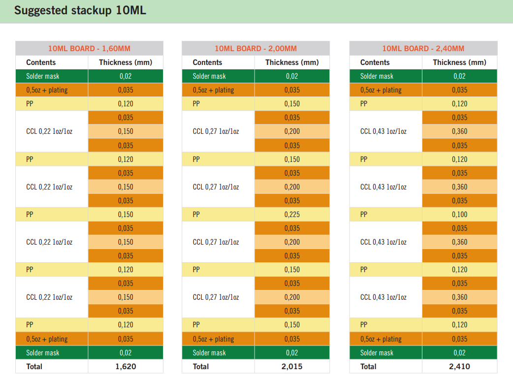
Design Tips – Stack-up
1. Ensure the stack-up remains symmetric.
2. Typically, a foil build is recommended. Special core builds, like those with Rogers, are possible but less common.
3. For boards thicker than 1mm, the standard thickness tolerance is +/-10%. For 1mm boards, the standard tolerance is +/-0.1mm. Any board with a thickness ≤1mm requires approval from Best Tech.
4. The minimum dielectric thickness will be 90µm, according to IPC standards, unless otherwise specified by the FAB drawing and there are no micro vias.
5. Use a maximum of three sheets of prepreg to bond the layers.
6. While the stack-up used in production may differ slightly from the specified one, an Engineering Query (EQ) will be sent for confirmation.
7. Variations can occur due to factors like copper distribution and available materials.
8. Thicker copper foils require thicker dielectrics between layers, and the foil thickness after processing differs from the base foil thickness.
9. Additionally, variations in resin percentage for the same prepreg type can impact the final prepreg thickness.
10. When incorporating micro vias, consider the aspect ratio—recommended at 0.8:1 and advanced at 1:1—when selecting prepreg.
If you need special materials, thickness tolerances, or stack-ups, contact Best Technology for guidance. Below are some suggested stack-ups for different layers PCB.
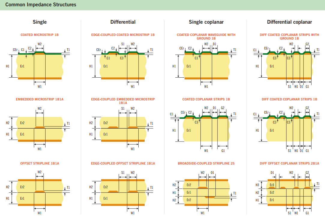
Impedance Parameters Needed for Calculation
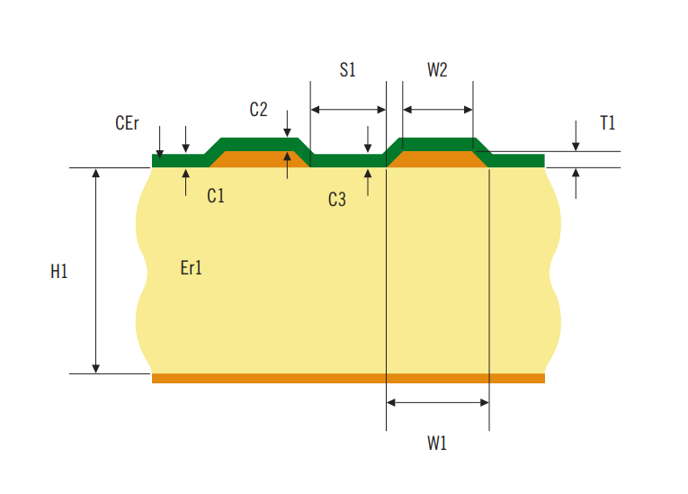
| Symbol | Feature |
| H1, H2, H3.. | Dielectric thickness between copper layers after pressing |
| Er1 | Dielectric constant of prepreg or core used between copper layers. |
| W1 | The bottom width od impedance lines, which is the customer required impedance trace width. |
| W2 | The top width of impedance lines. |
| S1 | The space between two differential impedance traces. |
| T1 | Finished copper thickness, which is different with our normal definition. |
| C1 | Solder mask thickness on material. |
| C2 | Solder mask thickness on copper. |
| C3 | Solder mask thickness on material between traces (C1 = C3). |
| CEr | Dielectric constant of solder mask. Normally use 3.4 to calculate. |
Tolerance of Impedance Control
| Type of Impedance | Common Requested Value | Tolerance of Impedance Control | ||
| General | Moderate | Advanced | ||
| Single/Single Coplanar | 40Ω/510Ω/75Ω | +/-10% | +/-8% | +/-5% |
| Differential/Differential Coplanar | 90Ω/100Ω/120Ω | +/-10% | +/-8% | +/-5% |
Relationship between Parameters and Impedance Value
| Parameters Modification | Effect on Impedance Value | ||
| Parameters | Increase/Reduce | Impacts on impedance | Impedance value increase/reduced |
| H (dielectric thickness) | Increase | Big | Increase |
| W (trace width) | Increase | Big | Reduced |
| S (trace space) | Increase | Big | Increase |
| T (copper thickness) | Increase | Low | Reduced |
| C (solder mask thickness) | Increase | Low | Reduced |
Design tips – Impedance
When signal speeds exceed 2 GHz and timing is critical, consider using better materials such as medium, high, or ultra-high-speed options, along with flat glass styles. To ensure a reliable lamination process and prevent resin starvation, allow the factory to select the number of prepregs, prepreg styles, and resin content in the stack-up.
Key factors influencing impedance signal losses include:
1. Line Length: Signal losses are directly proportional to the line length—shorter lines result in fewer losses, while longer lines lead to greater losses.
2. Dielectric Loss: These losses can be minimized by selecting appropriate materials.
3. Copper Loss: This includes losses from the cross-sectional area (affected by stack-up design) and surface roughness, which can be reduced through material selection and proper stack-up configuration.
If you require impedance tolerances tighter than +/-10%, discuss your design possibilities with the Best Technology team.
When designing rigid-flex boards, note that separate calculations are necessary for both the rigid and flex sections of the same signal. Manufacturers will adjust the thickness and dielectric constant of the solder mask based on their solder mask properties and printing method. Variations in resin content for the same prepreg type can also affect impedance. For assistance with impedance calculations, contact Best Technology for support.
Checklist of Necessary Information for Impedance Calculations
1. Specify the type, value, and tolerance of impedance control.
2. Ensure you define the width and space of impedance traces, as well as the layers where these traces will be present, along with the layers to be considered as reference points.
3. Identify the type of material and final board thickness, and provide a reference stack-up for the design.
4. Confirm the finished copper thickness on external and internal layers, and note if any special type of solder mask is required.
5. Always request Best Technology’s stack-up before starting the routing design.
You may also like


Tags: pcb design, pcb stackup