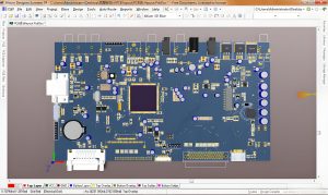
PCB is an important component of electronic equipment and comes in many types. Before the advent of printed circuits, electronic components were soldered together by hand, which led to manufacturing errors and resulted in bulky products with complex internal connections due to the large number of wires required.
Developments in printed circuit technology have facilitated more efficient and reliable design and manufacturing of electronic products, allowing for the precise arrangement of electronic components on small, compact circuit boards.
What are the advantages of PCB?
Miniaturization and lightweight: As consumer electronics products increasingly pursue portability and compact design, thin PCBs have become a key factor in achieving device miniaturization, which can significantly reduce the thickness and weight of the device, making the product more in line with modern aesthetics and use. Habit.
Improved heat dissipation performance: Thin PCB has a smaller heat capacity, which helps to quickly dissipate the heat generated by electronic components, thus improving the overall heat dissipation efficiency of the device.
Reduced production costs: Thin PCBs require relatively less raw materials during the manufacturing process, and coupled with the possible reduction in the number of assembly layers, the material cost per unit area is reduced.
Adapt to high-speed signal transmission: Due to its low dielectric loss, thin PCB can effectively reduce signal transmission delay, improve signal integrity, and meet the needs of high-speed data transmission.

High-density integration capability: PCB multi-layer boards allow for higher-density circuit layouts in a limited space. By arranging conductive paths and components between multiple layers, the size of the circuit board can be greatly reduced and electronic equipment can be improved. overall performance.
What are the disadvantages of PCB?
Mechanical strength problem: The mechanical properties of thin PCB are relatively weak, and it is easy to deform or break due to improper stress during assembly, transportation and even daily use.
Increased processing difficulty: Thin PCBs place higher requirements on the production process. Processes such as drilling, etching, and lamination need to be precisely controlled to prevent problems such as warping and breakage of thin plates.
Electromagnetic compatibility challenges: Thin PCB may increase parasitic capacitance and inductance, affecting the electromagnetic compatibility of the circuit.
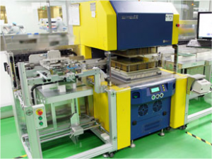
Higher manufacturing costs: The manufacturing process of multi-layer boards involves complex processes such as multiple laminations, drilling, and electroplating, resulting in relatively high production costs.
Long production cycle: Due to the complex production process of multi-layer boards, the production cycle is usually longer than that of single-layer or double-layer boards, which may affect the product’s time to market and market competitiveness.
As an indispensable basic material in electronic manufacturing, PCB has the advantages of high reliability, high precision, and small size, but it also has disadvantages such as design and cost restrictions. When choosing to use PCB, you need to comprehensively consider its advantages and disadvantages as well as specific application scenarios.
What are the limitations of PCB?
The limitations of PCB (Printed Circuit Board) mainly include the difficulty of design and manufacturing, complex testing and troubleshooting, and environmental impact.
Design and manufacturing are difficult: Designing multi-layer PCBs requires highly specialized knowledge and software tools to ensure signal integrity and optimization of power distribution.
Complex testing and troubleshooting: Due to the complexity of the multi-layer structure, once a failure occurs, it becomes more difficult and time-consuming to locate and repair the problem.
Environmental impact: Special chemicals and precious metals may be used in the production process of high-end multi-layer PCBs. If not handled properly, they may have a certain impact on the environment.
These limitations have put forward higher requirements for the design, manufacturing, testing and use environment of PCB, which require comprehensive consideration and optimization in terms of technology, cost, environmental protection and other aspects.
Why do PCB boards fail?
1. Improper design
Including unreasonable PCB board design, improper part orientation design, automatic plug-in bent legs, etc. These problems may lead to short circuit faults, and the part orientation or design needs to be modified to avoid short circuits.
2. Poor manufacturing
Problems during the manufacturing process, such as solder joint problems, damaged pads, improper installation of components, etc. These problems will affect the reliability of the welding and cause the circuit board to deform or crack.
3. Poor usage environment
PCB boards are affected by the environment, such as extreme temperature changes, excessive humidity, high-intensity vibration, etc., which may cause damage to the PCB board and affect its performance and reliability.
4. Other reasons
It also includes circuit board aging, design defects, manufacturing process problems, etc., such as metal components on the circuit board reacting with oxygen, causing oxidation, or assembly deviations during the manufacturing process causing component position deviation, etc.
What can damage a PCB?
Factors that damage PCB (Printed Circuit Board) mainly include physical damage, chemical corrosion, electrochemical corrosion, electrostatic discharge, humidity and moisture, temperature changes, etc.
1. Physical damage: including vibration, falling, hitting, and stacking, which may cause PCB deformation and cracks, leading to circuit breakage or short circuit.
2. Chemical corrosion: The PCB surface may be exposed to chemicals, such as acids, alkalis or other corrosive solutions, causing corrosion.

3. Electrochemical corrosion: When there is a potential difference between different metal components, a battery is formed in a humid environment, which accelerates the corrosion of one of the metals. This is called electrochemical corrosion.
4. Electrostatic discharge: Electrostatic discharge is the invisible killer of PCB. It can generate thousands of volts in an instant, which is enough to damage the components on the PCB.
5. Humidity and moisture: Extreme temperatures or temperature changes, as well as moisture in the air, can cause PCB board damage, such as deformation, short circuit, corrosion and other problems.
6. Temperature changes: Temperature changes can also cause solder joints, substrate materials and even casings to crack. If the circuit is going to be exposed to high temperatures, you may need to choose components that can withstand higher temperatures.
What is the lifespan of a PCB?
There is no fixed international standard for the service life of PCB, and its specific life span depends on many factors.
Materials and manufacturing processes: The materials and manufacturing processes of the PCB board have a decisive impact on its service life. PCB boards made of different materials and processes have different service lives.
Normal use and maintenance: Under normal use and no damage, the life of the circuit board itself is quite long. Manufacturers usually give a lifespan indicator of about 5 years, but this does not mean that the circuit board cannot be used after 5 years. In fact, as long as a circuit board is properly maintained and maintained, it can last for decades.
Lifetime under specific conditions: For PCBs containing OSP parts, the vacuum seal is valid for up to 3 months. For non-OSP PCBs, if the storage period exceeds 6 months but is less than one year, the chip factory will bake them before producing them; if the storage period exceeds one year, they will be scrapped. Boards opened during production should be used within 24 hours.
The service life of PCB is not a fixed value, but depends on the specific situation. With proper design, manufacturing, use and maintenance, the life of a PCB can be significantly extended.
What are the dangers of PCB?
The wastewater generated during the PCB manufacturing process contains heavy metals (such as copper, nickel, lead, etc.) and organic matter. If these pollutants are discharged without proper treatment, they will cause serious pollution to the environment.

In electronic products, common defects in PCB boards include open circuits, short circuits, false soldering, solder beads, and substrate warping. These defects can cause electronic products to fail to work properly or even fail completely.
PCB circuit boards play a vital role in the manufacture of modern electronic devices. They are widely adopted for their high reliability, compactness, and high scalability. When choosing to use PCB circuit boards, you need to consider their advantages and disadvantages and make a wise decision based on the needs of the specific project.
BEST Technology has been deeply involved in the circuit board industry for many years and has many solutions for various PCB problems. You can find us for all your PCB problems.