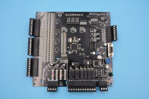
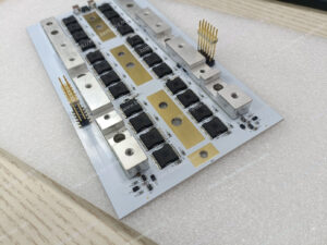
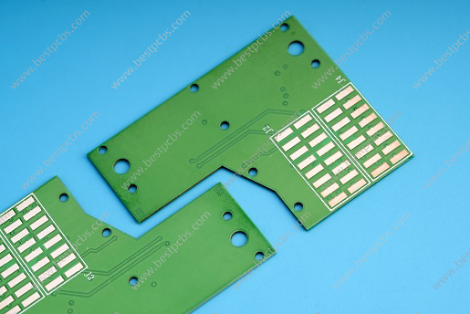
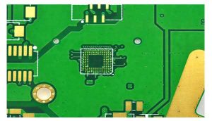
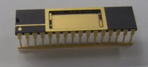
Thick film and thin film technologies for ceramic circuit boards each have their specific uses. The application of thick film technology is mainly concentrated in areas that require high reliability and high performance, such as the automotive field, consumer electronics, communications engineering, medical equipment, aerospace, etc.
The application of thin film technology focuses on products that require specific optical, electrical, chemical and thermal properties, such as reflective coatings, optical recording media, insulating films, anti-oxidation, sensors, optoelectronic device heat sinks, etc. The following will introduce the uses and differences of thick film and thin film one by one.
What is a thick film ceramic circuit board used for?
Thick film ceramic circuit board is a kind of circuit board made by thick film technology, which is widely used, mainly for electrical connection, component mounting and surface modification.
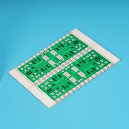
- Electrical connection
Thick film circuit board can effectively connect all parts of the circuit to ensure the smooth transmission of current.
- Component mounting
It can bear and fix electronic components, and ensure the correct position and stable operation of components in the circuit.
- Surface modification
Through thick film technology, the surface of the circuit board can be modified to improve its electrical performance and durability.
In addition, the thick film ceramic circuit board has some specific advantages, such as its manufacturing method allows it to be manufactured independently without using a substrate, and its thickness is usually between 10 and 25 μ m. This technology can be manufactured independently without using a substrate, which provides greater design flexibility. However, there may be some limitations in the accuracy of thick-film ceramic circuit boards. For example, in the process of using screen printing technology, the line width and accuracy may be insufficient due to the problems of screen printing, which may gradually lose the accuracy advantage for heat sinks with smaller and smaller size requirements in the future.
What is a thin film ceramic circuit board used for?
Thin film ceramic circuit boards are mainly used in module components of microwave circuits, including thin film load, thin film equalizer, thin film power divider, thin film attenuator, thin film coupler and thin film bridge.
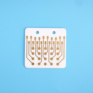
1. Thin film load is often used to match the terminals of module components of microwave circuits to absorb redundant incident power. It is designed with alumina ceramic substrate, which has the advantage of high precision machining.
2. Thin-film equalizer is used to adjust the broadband power flatness of microwave circuits. By changing the square resistance of the integrated tantalum nitride film and designing different resistance values, the output waveform of the device is adjusted to achieve the balance of power signals.
3. Thin film power divider is used in multi-channel communication network system, which distributes power according to a certain proportion, and one input can be multi-output, thus avoiding the problem of unstable patch resistance welding of microstrip power divider.
4. Thin film attenuator is used for large signal attenuation or multi-gear adjustment attenuation value in microwave RF module, which realizes high attenuation value flatness of ultra-wideband and stable performance.
5. Thin-film couplers are used for power detection or signal separation, and can be designed as couplers with any weak coupling degree. tantalum nitride design is used to integrate isolated loads, which is suitable for broadband applications.
6. As a part of microwave module, thin film bridge is used for specific circuit connection and signal processing.
According to these applications, we can better understand the wide application and advantages of thin-film ceramic circuit boards in the fields of high frequency, high power and high integration.
What are the advantages of thick film over thin film ceramic PCB?
Thick film ceramic circuit boards have higher mechanical strength and thermal conductivity than thin film ceramic circuit boards, and are more suitable for power electronics, automotive electronics and other occasions that require higher thermal management and mechanical strength.
The main difference between thick-film ceramic circuit board and thin-film ceramic circuit board lies in their film thickness and manufacturing process. The thickness of thick film circuit board is generally greater than 10μm, while that of thin film circuit board is mostly less than 1μ m.. Thick film circuit board usually adopts screen printing process, while thin film circuit board adopts vacuum evaporation, magnetron sputtering and other process methods.
This difference in technology leads to their differences in performance and application fields. Specifically, the advantages of thick film ceramic circuit boards are mainly reflected in the following aspects:
Reliable performance
Thick film circuits are flexible in design, low in investment and cost, and are mostly used in high voltage, high current and high power occasions.
High mechanical strength
Due to the use of thick film materials, thick film ceramic circuit boards have high mechanical strength and can withstand greater physical pressure and impact.
Good thermal conductivity
Thick-film ceramic circuit boards have good thermal conductivity, which is conducive to rapid heat dissipation, and is particularly important for electronic equipment that needs good thermal management.
Therefore, thick film ceramic circuit boards are more suitable for applications that require high mechanical strength and good thermal conductivity, such as power electronics, automotive electronics and other fields.
What is the difference between thick film and ceramic resistors?
There are some differences between film resistance and ceramic resistance in materials, manufacturing technology, size and shape, electrical properties and application scenarios.
1. Materials and manufacturing process: Thick film resistors are usually made by screen printing process and spraying or sputtering on the circuit substrate. The commonly used substrate materials are ceramics, glass and so on. The ceramic resistor is a resistance device made of ceramic material, which is fired in a ceramic kiln.
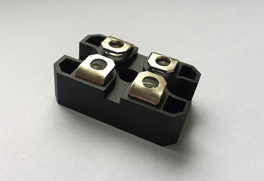
2. Size and shape: Thick film resistors are usually flat, can be made into various sizes and shapes, and are suitable for assembly on circuit boards. Ceramic resistors are usually cylindrical and have a fixed size and shape.
3. Electrical performance: Thick film resistor has high resistance accuracy and stability, and small temperature coefficient. Ceramic resistors have larger power carrying capacity and higher withstand voltage.
4. Application scenario: Thick film resistor is suitable for high-precision circuits because of its large resistance range and good temperature stability. Ceramic resistors are suitable for general circuits and small electronic devices because of their small size and general electrical properties.
From this, we can know that thick film resistors and ceramic resistors are different in materials, manufacturing processes, sizes and shapes, electrical properties and application scenarios, which make them suitable for different electronic equipment and circuit design requirements.
Thick film technology and thin film technology have certain substitutability in some fields, but thick film technology has irreplaceable role in the manufacturing and related processes of many products due to its advantages in cost, reliability, high temperature performance, etc., especially in multi-layer co-sintering processes such as LTCC and HTCC, where thin film technology cannot be applied. As a professional ceramic substrate manufacturer, Best Technology is committed to providing customers with high-quality thick film and thin film ceramic substrates to meet the needs of different applications.
Tags: ceramic circuit board, thick film ceramic resistor, thick fim ceramic pcb


