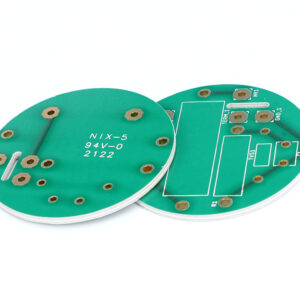
Copper weight refers to the amount of copper per square foot of the PCB surface, measured in ounces per square foot (oz/ft²). However, the term “copper thickness” is also commonly used. So, how do copper weight and thickness relate to each other?
Copper thickness is determined by rolling a specific weight of copper over a 1 square foot area. For instance, if 1 ounce of copper is spread out over an area of 1 square foot, the resulting thickness of the copper foil is approximately 1.37mils or 0.0348mm.
What is the Standard Copper Weight for PCB?
The standard copper weight in PCBs typically ranges from 1 oz/ft² to 3 oz/ft². This measurement refers to the weight of copper per square foot. In metric terms, it translates to approximately 35 µm to 105 µm thickness. The choice of copper weight depends on the application and the current-carrying requirements of the PCB. For standard consumer electronics, 1 oz/ft² is often sufficient. However, power electronics and high-current applications may require heavier copper.
What is Copper Thickness in PCB?
PCB typically feature a layer of copper foil bonded to a glass epoxy substrate. Common copper foil thicknesses are 18μm, 35μm, 55μm, and 70μm. The most frequently used thickness is 35μm. In practice, copper foil thicknesses used domestically generally range from 35μm to 50μm, with thinner options like 10μm or 18μm and thicker options like 70μm also available.
For substrates that are 1mm to 3mm thick, the copper foil is typically 35μm thick. On substrates less than 1mm thick, the copper foil is about 18μm thick, while on substrates thicker than 5mm, the copper foil is around 55μm thick.
If a PCB has a copper foil thickness of 35μm and a trace width of 1mm, the resistance per 10mm length of the trace is approximately 5mΩ, and the inductance is about 4nH. When a digital integrated circuit on the PCB operates with a di/dt of 6mA/ns and a current of 30mA, the estimated noise voltage generated in the circuit due to resistance and inductance for every 10mm length of the trace is 0.15mV and 24mV.
Copper Weight vs. Copper Thickness
Here’s a chart illustrating the relationship between copper weight, copper thickness in mils, and copper thickness in millimeters (mm).
| Copper Weight (oz/ft²) | Copper Thickness (mils) | Copper Thickness (mm) |
| 0.5 | 0.7 | 0.018 |
| 1 | 1.4 | 0.035 |
| 2 | 2.8 | 0.070 |
| 3 | 4.2 | 0.105 |
| 4 | 5.6 | 0.140 |
| 5 | 7.0 | 0.175 |
| 3 | 8.4 | 0.210 |
How Do You Calculate Copper Weight in PCB?
Calculating copper weight involves determining the thickness of the copper layer. Here’s a simple method:
- Measure the thickness of the copper in micrometers (µm).
- Use the conversion factor: 1 oz/ft² equals 35.56 µm.
- Multiply the thickness by the conversion factor to get the weight in oz/ft².
For example, if the copper thickness is 70 µm, the calculation is:
Copper weight (oz/ft²)=70um/35.56um/oz≈2oz/ft2
You can use a PCB weight calculator to simplify this process, like PCBWay Calculator, Altium PCB Layout Weight Calculator.
How Much Copper is in a PCB?
The amount of copper in a PCB varies depending on the copper weight and the size of the board. For instance, a 10 cm x 10 cm PCB with a copper weight of 1 oz/ft² will have less copper than the same size board with 3 oz/ft² copper weight. To estimate the total copper, you need to know the board area and the copper thickness.
Total copper (grams)=Area (cm²)×Copper thickness (µm)×8.96×10⁻³
The factor 8.96 x 10^-3 converts the volume to weight, considering copper’s density.
What is the Density of Copper in PCB?
Copper’s density is a constant value of 8.96 g/cm³. This density is crucial for calculating the weight of copper in a PCB. Knowing the density helps in accurately estimating the amount of copper in your PCB, which is essential for both design and manufacturing processes. The density remains constant regardless of the copper weight or thickness, providing a reliable basis for various calculations in PCB design.
Why Copper Thickness is Important for PCB?
In the PCB manufacturing process, copper thickness is a very important factor. The correct copper thickness can ensure the quality and performance of the circuit board, but also ensure the reliability and stability of electronic products. We have listed the following points to show why copper thickness is so important for PCBs.
1. Electrical conductivity
Copper thickness determines the electrical conductivity of the circuit board. As you know, copper is an excellent conductive material, and its thickness directly affects the conductive effect of the circuit board. Thinner copper layer may reduce the electrical conductivity of PCB, and resulting in attenuation of signal transmission or instability of current. And if the copper layer is too thick, although the electrical conductivity will be very good, but will increase the cost and weight of the circuit board. Additionally, thicker copper thickness is easy to lead to serious glue flow, the medium layer is too thin, and increase the manufacturing process difficulty. Therefore, for normal PCB, the copper thickness is generally not recommended to do 2oz copper thick, otherwise you can choose Heavy Copper PCB.
2. Heat dissipation
Copper thickness also has an important impact on the heat dissipation performance of the circuit board. The copper layer is the thermal conductivity layer of the circuit board, and its thickness determines the heat dissipation effect. If the copper layer is too thin, it may cause heat to be unable to conduct and dissipate effectively, increasing the risk of overheating of components. Therefore, the copper thickness of the PCB cannot be too thin, in the PCB design process, we can also lay copper in the blank area to assist the heat dissipation of the PCB board.
3. Improve reliability
Copper thickness also has an important impact on the reliability and stability of the circuit board. The copper layer not only acts as the conductive layer and thermal layer, but also the support and connection layer of the circuit board. The appropriate copper thickness provides sufficient mechanical strength to prevent the board from bending, breaking, or opening welding during use. At the same time, the appropriate copper thickness can ensure the welding quality of the circuit board and other components, reducing the risk of welding defects and failures.
How to Select Suitable Copper Weight for PCB?
Selecting the suitable copper weight depends on several factors:
- Current Carrying Capacity
Higher currents require thicker copper to prevent overheating. Calculate the required trace width and copper thickness based on the maximum current your PCB will carry.
- Thermal Management
Thicker copper improves heat dissipation, essential for high-power applications. Consider the thermal requirements of your components and ensure the PCB can manage the heat effectively.
- Mechanical Strength
Heavier copper can enhance the board’s structural integrity. For applications where the PCB will face mechanical stress or flexing, thicker copper provides added durability.
- Cost Considerations
Thicker copper increases material costs, so balance performance needs with budget constraints. While thicker copper offers many benefits, it also comes with higher manufacturing costs. Evaluate whether the additional expense is justified for your specific application.
- Signal Integrity
For high-frequency applications, maintaining signal integrity is crucial. Thicker copper can help reduce resistance and signal loss, improving overall performance.
- Environmental Factors
Consider the operating environment of the PCB. For harsh conditions, thicker copper may offer better protection against corrosion and environmental stressors.
For most applications, 1 oz/ft² copper is adequate. For power electronics or where higher currents are involved, consider 2 oz/ft² or more. Consult with your PCB manufacturer for recommendations based on your specific use case. They can provide insights into the optimal copper weight for your design, considering both performance and cost-effectiveness.


