The full form of BGA is Ball Grid Array. BGA is one of the most important elements in the electronic device. From smartphones to advanced computing systems, BGA electronics are everywhere. In this article, we will discuss what a BGA is? How does it work and its advantages & disadvantages in the modern electronics.
What is a BGA in PCB?
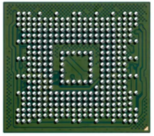
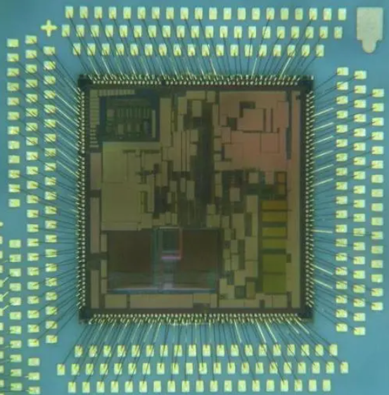
Ball grid Array (BGA) is a surface-mount package used to attach integrated circuits (ICs) to printed circuit boards (PCBs) to permanently protect devices such as microprocessors. Unlike the older through-hole method, BGA utilizes tiny solder balls that are arranged in a grid at the bottom of the IC package. These solder balls allow for more efficient connection to the PCB. BGA packages can accommodate more pins than other packages, such as Dual In-line Packages (DIP) or Quad Flat packages (QFP), and the entire underside of the device can be used as a pin, not just around it. It also has a shorter average line length than the package types defined around it for better high-speed performance.
These solder balls can be configured manually or by automated machines and positioned by flux. When the device is fixed on the PCB by surface bonding technology, the arrangement of the bottom tin balls exactly corresponds to the position of the copper foil on the board. The production line then heats it up, either in a reflow oven or an infrared oven, to dissolve the tin balls. The surface tension causes the melted tin balls to hold the seal and align to the board. At the correct spacing, when the tin balls are cooled and fixed, the welded contacts are formed to connect the device to the PCB.
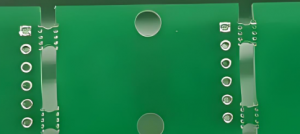
PCB boards with BGA generally have many via holes. Generally, the holes under the BGA chip is designed as a finished hole, with a diameter of 8~12mil. They need to be plugged, no ink and no drilling is allowed on the pad.
How does BGA works?
BGA works by replacing the traditional leads used in older packages with a grid of solder balls. When the IC is mounted to the PCB, the solder balls are heated, causing them to melt and create electrical connections. These connections ensure that the IC functions as intended by linking it directly to the board’s circuitry. The grid arrangement not only makes it possible to pack more connections into a smaller area but also improves the thermal performance, allowing heat to dissipate more efficiently. BGA ICs are thus more reliable and efficient in high-performance applications.
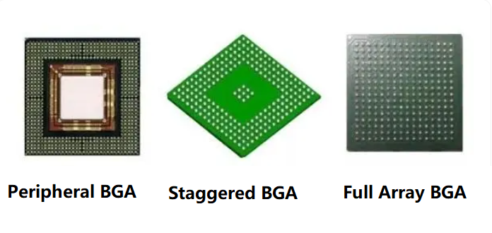
Types of BGA packages
There are many types of BGA packages, which can be categorized based on the arrangement of the solder balls into peripheral, staggered, and full array types. According to the different substrates, the main categories include PBGA (Plastic BGA), CBGA (Ceramic BGA), FCBGA (Flip-chip BGA), and TBGA (Tape BGA). Let’s explain different types of BGAs in detail.
1. PBGA Package
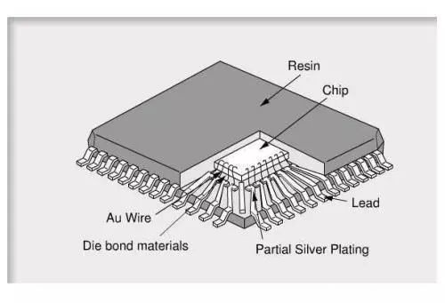
PBGA is the most commonly used BGA packaging type, made using plastic materials and plastic processes. The substrate used is PCB substrate material (BT resin/glass laminate). The bare chip is attached and connected to the top of the substrate and the lead frame using bonding and WB technology, followed by molding through the injection process (epoxy film/plastic mixture). Intel CPUs, including Pentium II, III, and IV processors, use this packaging type.
The solder ball material is a low-melting-point eutectic solder alloy 63Sn37Pb, with a diameter of about 1mm and a spacing range of 1.27-2.54mm. The connection between the solder balls and the bottom of the package does not require additional solder. During assembly, the solder balls melt, joining with the PCB surface pads, forming a barrel shape.
Features of PBGA packaging
- Low production cost, high cost-effectiveness.
- The solder balls participate in the reflow soldering joint formation, and the coplanarity requirements are relatively loose.
- Good thermal compatibility with epoxy resin substrates, ensuring high quality and performance when assembled onto PCBs.
- Sensitive to moisture, with a serious PoPCorn effect, which presents reliability issues. The height of the package is also a technical challenge compared to QFP.
2. CBGA Package
CBGA involves mounting the bare chip on the top surface of a ceramic multilayer substrate. A metal cover plate is soldered onto the substrate using sealing solder, protecting the chip, leads, and pads. The connected package undergoes hermetic sealing to improve reliability and physical protection. Pentium I, II, and Pentium Pro processors have used this packaging type. CBGA employs multilayer ceramic wiring substrates, with the solder ball material being high-melting-point 90Pb10Sn eutectic solder. The connection between the solder balls and the package is made using low-temperature eutectic solder 63Sn37Pb, with a sealed cap and glass hermetic sealing, placing it in the hermetic packaging category.
Features of CBGA packaging
- Not sensitive to moisture, high reliability, and excellent electrical and thermal performance.
- Good CTE compatibility with ceramic substrates.
- Better reworkability for connecting chips and components.
- The bare chip uses FCB technology, allowing for higher interconnection density.
- Higher packaging cost.
- Poor CTE compatibility with substrates like epoxy resin.
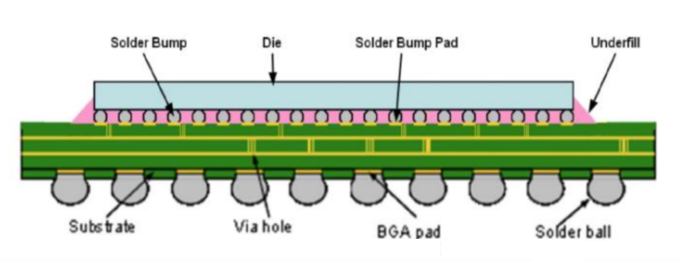
3. FCBGA Package
FCBGA is currently the main packaging format for graphics accelerator chips. This packaging technology originated in the 1960s when IBM developed the so-called C4 (Controlled Collapse Chip Connection) technology for large computer assembly. It was later developed further to utilize the surface tension of molten bumps to support the chip’s weight and control the bump height, becoming a direction in flip-chip technology development.
This packaging uses small balls instead of pins to connect the processor. A total of 479 balls are used, each with a diameter of 0.78mm, providing the shortest external connection distance. FCBGA connects the chip to the substrate using FCB technology, differing from PBGA in that the bare chip faces downward.
4. TBGA Package
TBGA, also known as Tape Ball Grid Array, is a relatively novel BGA packaging format. It uses PI multilayer wiring substrates, and the solder ball material is high-melting-point solder alloy, with low-melting-point solder alloy used during welding.
Advantages of BGA
- BGA packages are smaller in size compared to SOP packages. For the same memory IC and capacity, the volume of a BGA is only one-third that of an SOP package.
- In QFP and SOP packages, the leads are distributed around the perimeter of the package. As the number of leads increases, the spacing decreases, making the leads prone to deformation and bending. In contrast, BGA solder balls are located on the bottom of the package, and the spacing is larger, significantly improving the yield rate.
- BGA leads are very short, using solder balls instead of wires. The signal path is short, reducing inductance and capacitance, which enhances electrical performance.
- The spherical contact array and the gap formed with the substrate improve heat dissipation from the package body.
- BGA body and PCB board have good coplanarity, can effectively ensure the quality of welding.
Disadvantages of BGA
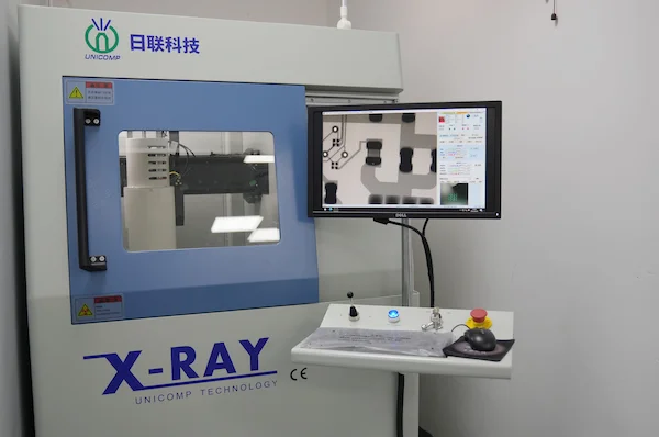
- After soldering, it is difficult to inspect and repair BGA packages. X-ray inspection is required to ensure the electrical performance of the solder joints. Quality cannot be determined through visual inspection or Automated Optical Inspection (AOI).
- Since the BGA pin is at the bottom of the body, which is easy to cause welding shadow effect, so the welding temperature curve is higher. The actual welding temperature must be monitored in real time.
- If individual BGA solder joints are faulty, the entire BGA package must be removed, re-balled, and then resoldered. This affects the throughput rate and electrical performance.
- BGA packages are more robust compared to QFP packages with 20 mil spacing. BGAs do not have leads that can bend or break. Soldering is secure, and if the BGA needs to be removed, a high-temperature rework station must be used.
What is the difference between BGA and FPGA?
BGA refers to a packaging type, while FPGA is a type of semiconductor device that can be programmed after manufacturing. An FPGA can be packaged in a BGA format, but they are not the same thing.
FPGA is further developed on the basis of traditional logic circuits and gate arrays such as PAL (Programmable logic Array), GAL (universal array logic), CPLD (complex programmable logic device). It uses computer-aided design to draw the schematic diagram, edit Boolean equation or use hardware description language as design input. Then through a series of conversion programs, automatic layout and wiring, simulation and simulation process; Finally, the data file of FPGA is generated and the FPGA device is initialized. In this way, the ASIC that meets the requirements of users is realized, and the purpose of designing, developing and producing integrated circuits by users is truly achieved.
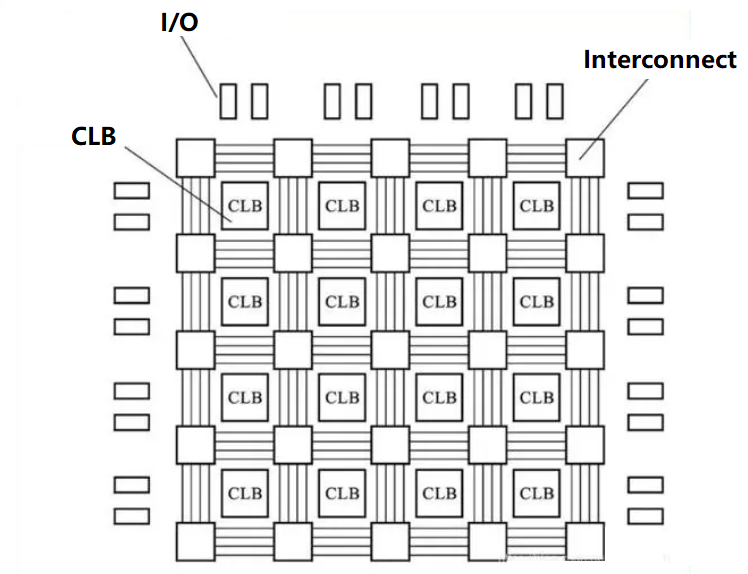
FPGA consists of programmable logic block (CLB), input/output module (IOB), programmable Interconnect resource (PIR) and static memory SRAM used to store programming data. CLBS are the basic units that implement logic functions, and they are usually arranged in a regular array, scattered throughout the chip. The IOB mainly completes the interface between the logic on the chip and the external pins, and is usually arranged around the chip. PIR provides a wealth of connection resources, including crossbar mesh connections, programmable switch matrices, and programmable connection points, which connect individual CLBS, CLBS and IOBs, and IOBs to form circuits for specific functions. Static memory SRAM is used to store the programming data of internal IOB, CLB and PIR, and form the control of IOB, CLB and PIR, so as to complete the system logic function.
If you want to know more about BGA, welcome to leave your message below.