

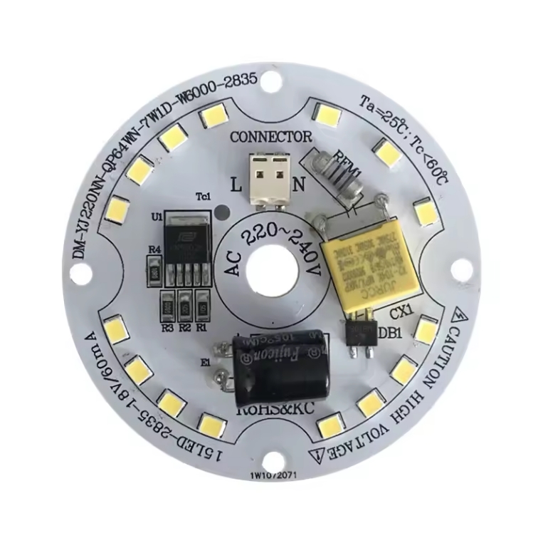
led light pcb , or printed circuit board, is a stable carrier of electronic components. It not only realizes electrical connection but also plays a supporting role. As the core component of electronic products, it is widely used in various electronic devices. In the field of LED lighting, PCB light board provides support and power for LED lamp beads, ensuring their stable operation in scenes such as home, commercial and automotive lighting. PCB with LED is often used to manufacture electronic products such as indicator lights, lighting equipment and display screens. The LED lamp beads on these PCBs are usually precisely soldered by SMT (surface mount technology).
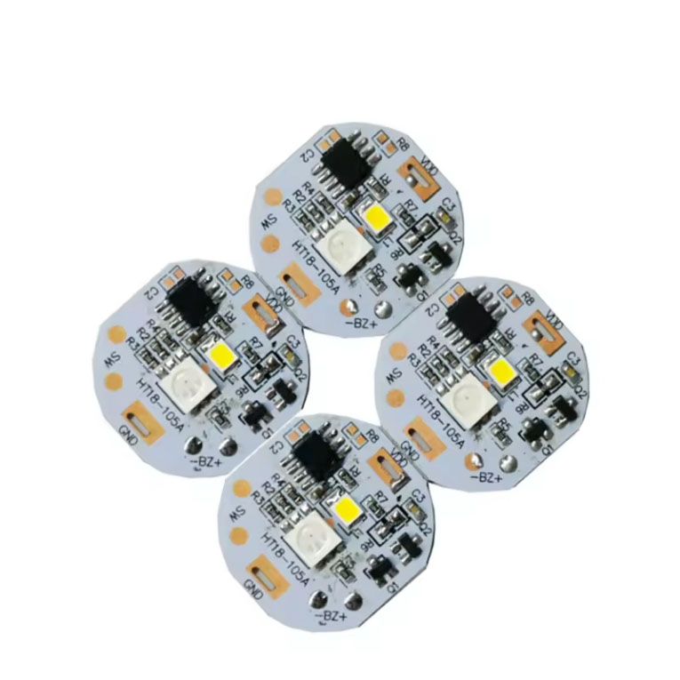
led light pcb
LED PCB light board leads the development of the lighting industry with its innovative design, high efficiency and flexibility, bringing a more intelligent and comfortable lighting experience to our lives. It is not only an integrated platform for electronic components, but also a perfect combination of modern technology and aesthetics, and is the focus of future lighting trends.
Why use mcpcb for led light pcb
With the continuous development of LED technology, the heat generated by LEDs has gradually increased. The traditional FR4 printed circuit board (PCB) has been unable to meet the heat dissipation requirements due to its low thermal conductivity (only 0.36W/m.K). In order to solve this problem, the metal core printed circuit board (MCPCB) was proposed. It attaches the original printed circuit board to a metal with better thermal conductivity (such as aluminum and copper) to enhance the heat dissipation effect. The thermal conductivity efficiency of MCPCB is higher than that of traditional FR4 PCB, reaching 1W/m.K to 2.2W/m.K, which effectively improves the heat dissipation performance of LED PCB.
In addition, the use of MCPCB can also reduce the number of LEDs required to generate lighting, making it an ideal choice for street lights, automotive LED applications, and backlight unit applications. The use of metal substrates has practical advantages in heat dissipation, thermal conductivity, reliability, and electrical insulation, especially in harsh environments, and can also achieve reliable operation of LEDs. For example, using a metal substrate can reduce the LED junction temperature by 20-30°C, improve light output and enhance the overall performance of the product, ensure consistent UV light generation, and expand the possibilities of UV applications in various industries.
Why use mcpcb for led light pcb
Advantages of led light pcb?
High thermal conductivity: LED PCB, especially aluminum substrate, uses aluminum alloy material with high thermal conductivity, which can effectively conduct away the heat generated by LED, maintain the stability of LED operation and extend the service life. This high thermal conductivity is essential to prevent heat accumulation and keep LED working at high brightness for a long time.
High efficiency: Compared with traditional incandescent lamps and energy-saving lamps, LED lamps have higher luminous efficiency and can provide better lighting effects while reducing energy consumption. This makes LED PCB have significant advantages in energy saving and environmental protection.
Long life: The service life of LED PCB far exceeds that of traditional lighting products, and it can provide longer continuous lighting, reducing the trouble of frequent bulb replacement and reducing maintenance costs.
Low energy consumption: LED PCB requires much less electricity than traditional lighting equipment while providing the same brightness, which is very important for energy saving, emission reduction and sustainable development
How does led light pcb dissipate heat?
The power device is mounted on the circuit layer. The heat generated by the device during operation is quickly transferred to the metal base layer through the insulating layer, and then the metal base layer transfers the heat to achieve heat dissipation of the device. Compared with the traditional FR-4, the aluminum substrate can reduce the thermal resistance to the minimum, making the aluminum substrate have excellent thermal conductivity; compared with the thick film ceramic circuit, its mechanical properties are extremely good. In the circuit design scheme, the heat diffusion is handled very effectively, thereby reducing the module operating temperature, extending the service life, and improving the power density and reliability; reducing the assembly of the heat sink and other hardware (including thermal interface materials), reducing the product volume, and reducing the hardware and assembly costs; combining the power circuit and the control circuit
How to make a LED light circuit board?
- Cutting
- Cutting process Picking materials – cutting
- The purpose of cutting
Cut the large-sized incoming materials into the size required for production - Precautions for cutting
① Check the size of the first piece of material
② Pay attention to the scratches on the aluminum surface and the copper surface
③ Pay attention to the delamination and flash of the board edge - Drilling
- Drilling process
Pinning – drilling – board inspection - The purpose of drilling
Positioning and drilling holes in the board to assist the subsequent production process and customer assembly - Precautions for drilling
① Check the number of holes and the size of the holes
② Avoid scratches on the board
③ Check the flash of the aluminum surface and the hole position deviation
④ Check and replace the drill bit in time
⑤ Drilling is divided into two stages, one drilling: drilling holes after cutting for peripheral tool holes
Second drilling: tool holes in the unit after solder mask - Dry/wet film imaging
- Dry/wet film imaging process
Grinding board – film pasting – exposure – development - Purpose of dry/wet film imaging
To present the part required for making circuits on the board - Precautions for dry/wet film imaging
① Check whether the circuit is open after development
② Whether the development alignment is biased to prevent the generation of dry film fragments
③ Pay attention to the circuit defects caused by scratches on the board
④ No air should remain during exposure to prevent poor exposure
⑤ After exposure, it should be still for more than 15 minutes before development
IV. Acid/alkaline etching - Acid/alkaline etching process
Etching-film stripping-drying-board inspection - Purpose of acid/alkaline etching
After imaging the dry/wet film, keep the required circuit part and remove the excess part outside the circuit. During acid etching, attention should be paid to the corrosion of the etching solution to the aluminum substrate; - Precautions for acid/alkaline etching
① Pay attention to incomplete etching and excessive etching
② Pay attention to line width and line thickness
③ Oxidation and scratches are not allowed on the copper surface
④ The dry film should be removed cleanly
V. Silk screen solder mask and characters - Silk screen solder mask and character process
Silk screen-pre-bake-exposure-development-characters - Purpose of silk screen solder mask and characters
① Anti-soldering: protect circuits that do not need soldering and prevent tin from entering and causing short circuits
② Characters: serve as markings - Precautions for silk screen solder mask and characters
① Check whether there is garbage or foreign matter on the board
② Check the cleanliness of the stencil ③ Pre-bake for more than 30 minutes after silk screen printing to avoid bubbles in the circuit
④ Pay attention to the thickness and uniformity of the silk screen
⑤ After pre-bake, the board should be completely cooled to avoid film contamination or damage to the glossiness of the ink surface
⑥ Place the ink side down during development
VI. V-CUT, gong board - V-CUT, gong board process
V-CUT——gong board——tear protective film——remove burrs - Purpose of V-CUT, gong board
① V-CUT: Cut the single PCS circuit and the entire PNL board to leave a small part connected for easy packaging and removal
② Gong board: remove the excess part of the circuit board - Precautions for V-CUT, gong board
① During the V-CUT process, pay attention to the size of the V, the incompleteness and burrs of the edges
② Pay attention to the burrs caused by the gong board, the gong knife is tilted, and the gong knife is checked and replaced in time
③ Finally, avoid scratches on the board when removing the burr
VII. Testing, OSP - Testing, OSP process
Circuit test-voltage resistance test-OSP - Testing, the purpose of OSP
① Circuit test: Check whether the completed circuit is working normally
② Voltage resistance test: Check whether the completed circuit can withstand the specified voltage environment
③ OSP: Allow the circuit to be soldered better - Testing, OSP precautions
① How to distinguish and store qualified and unqualified products after testing
② Placement after OSP
③ Avoid damage to the circuit
VIII. FQC, FQA, packaging, shipment - Process
FQC-FQA-packaging-shipping - Purpose
① FQC conducts full inspection and confirmation of the product
② FQA spot check and verification
③ Pack and ship to customers as required - Note
① FQC should pay attention to the appearance confirmation during the visual inspection and make reasonable distinctions
② FQA should conduct random inspections to verify the inspection standards of FQC
③ Confirm the packaging quantity to avoid mixed boards, wrong boards and packaging damage
Capabilities of led light pcb?
| Item | Capabilities |
| Layer Count | 1 – 10 Layers |
| Max Board Dimension | 24*64″(610*1625mm) |
| Min Board Thickness | 0.6mm |
| Max Board Thickness | 4.0mm |
| Conductor Thickness | 0.5oz – 10oz |
| Min Line Width/Line Space | 4/4mil (0.10/0.10mm) |
| Min Hole Diameter | 10mil (0.25mm) |
| Min Punch Hole Dia | 0.12″ (3.0mm) |
| Min Hole Spacing | 16mil (0.4mm) |
| Min PAD Ring(Single) | 3mil (0.075mm) |
| PTH Wall Thickness | Normal: 0.59mil (15um); HDI: 0.48mil (12um) |
| Min Solder PAD Dia | 14mil (0.35mm) |
| Min Soldermask Bridge | 8mil (0.20mm) |
| Min BAG PAD Margin | 5mil (0.125mm) |
| PTH/NPTH Dia Tolerance | PTH: ±3 mil (0.075mm); NPTH: ±2mil (0.05mm) |
| Hole Position Deviation | ±3mil (0.075mm) |
| Outline Tolerance | CNC: ±6 mil (0.15mm); Die Punch: ±6 mil (0.1mm) |
| Max Aspect Ratio | 10:01 |
| Surface Treatment | ENIG, Flash Gold, Hard Gold Finger, Gold Plating(50mil), Gold finger, |
| Selected Gold Plating, ENEPIG, ENIPIG, HAL, HASL(LF), OSP, Silver Imm., Tin Imm |
Applications of led light pcb?
- Application in medical equipment
The rapid progress of medicine is closely related to the rapid development of the electronics industry. Many medical devices are made of basic PCBs alone, such as pH meters, heart rate sensors, temperature measurements, electrocardiographs, electroencephalographs, MRIs, X-ray machines, CT scanners, blood pressure machines, blood sugar level measuring equipment, etc. - Application in industrial equipment
PCBs are widely used in manufacturing, especially in industries with high-power mechanical equipment; these devices run on high power and require high current circuit drive. Such as arc welding, large servo motor drives, lead-acid battery chargers, clothing cotton machines, etc. - Application in lighting
LED lights and high-intensity LEDs are mounted on PCBs based on aluminum substrates; aluminum has the property of absorbing heat and dissipating it in the air. - Application in the automotive and aerospace industries
Flexible PCBs are lightweight but can withstand high vibrations. Because of their light weight, they can reduce the total weight of spacecraft; flexible PCBs can be adjusted even in narrow spaces. These flexible PCBs are used as connectors, interfaces, and can be assembled even in compact spaces