

PCB test is a method of performing operational and functional tests on a circuit board and layout optimization. PCB test identifies any shorts, opens, incorrect component placement, or faulty components.
The purpose of PCB test and inspection is to check if the PCB meets the performance of a standard printed circuit board. It ensures that all PCB manufacturing processes are operating properly and without any defects as per the project specifications.
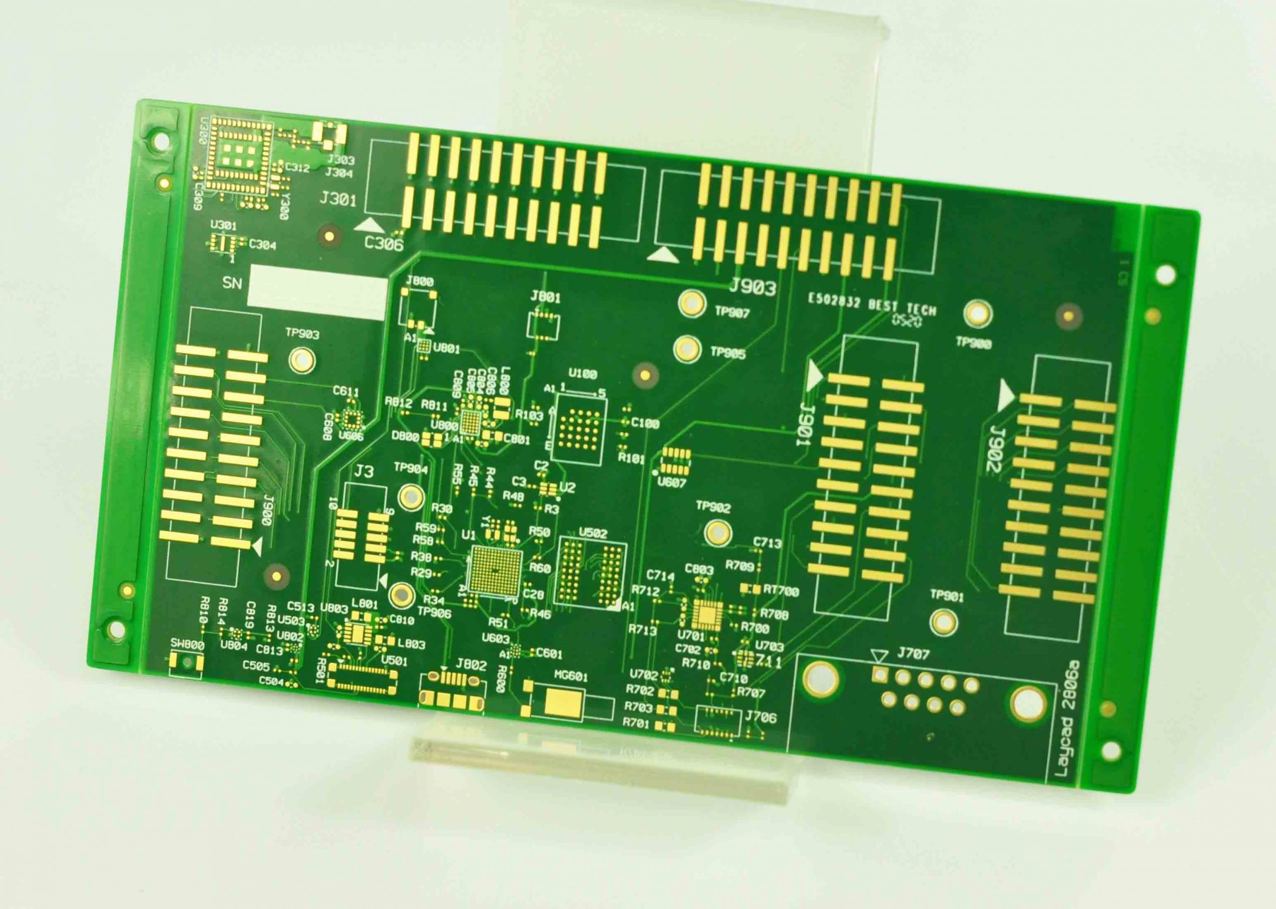
A PCB consists of different elements and components, each of which affects the overall performance of the electronic circuit. These components are analyzed in detail to ensure the quality of the PCB.
What is a PCB test?
PCB test is a technique that uses electronic testing instruments to detect the performance and quality of PCB (Printed Circuit Board) circuit boards. It is widely used in the electronics manufacturing industry to help manufacturers improve product quality and production efficiency.
The main purpose of PCB test is to ensure that all parts on the circuit board are properly connected and can still work properly under high voltage environments, while verifying whether the function of the circuit board is normal. Test methods include connectivity testing, withstand voltage testing, and functional testing, while inspection standards involve appearance inspection, size inspection, and performance inspection. In addition, PCB test also involves a series of professional techniques and methods, such as flying probe test, ICT test, FCT test, AOI test, etc., to ensure the electrical performance and structural integrity of the circuit board.
How to Test PCB?
PCB contains different components that affect the overall performance of electronic circuits. Tests are performed to check and optimize the status of these components using computerized machine software, simple electronic test equipment and tools, and even basic manual inspections.
1. Electrical test
2. Hole wall quality
3. Mechanical resistance test
4. Soldering quality
5. Cleanliness inspection, considering weather resistance, humidity and corrosion
6. Lamination, testing the ability of laminates to resist or heat peeling
Environmental testing is particularly necessary for PCBs used in humid environments.
What are the benefits of PCB test?
Error identification: The main benefit of PCB test is that it helps identify problems in PCBs. Whether the problem lies in functionality, manufacturability or other aspects, PCB test can identify problems in PCB design and layout.
Save time: Performing PCB test early helps save time in the long run by allowing designers to identify major issues during the prototyping phase. Comprehensive testing allows designers to quickly and easily identify the root cause of each issue and make adjustments so that they can move to production at a faster pace and reduce product lead times.
Reduce costs: PCB test avoids the waste of producing defective products by testing products using prototypes and small-scale components. By completing comprehensive testing early in the design process, designers can avoid the waste of producing defective PCBs, ensuring that the design is as perfect as possible before going into production.
Reduced returns: When PCB test is performed, the likelihood of selling defective products or products that do not meet performance standards is reduced, reducing the costs associated with refunding customers and handling defective goods.
Improved safety: Defective PCBs can cause fires, which can endanger people nearby. Pre-manufacturing testing also ensures that machines and workers are not damaged or injured due to poor design during the production process.
What are the types of PCB test?
1. In-circuit testing
In-circuit testing (ICT) is the most reliable type of PCB test available today. The high price reflects this – tens of thousands of dollars, although the cost depends on factors such as board and fixture size.
Also known as bed of nails testing, ICT fires and activates individual circuits on a board. In most cases, the test is designed to achieve 100% coverage, but actual coverage will be closer to 85-90%.
The test involves the use of fixed probes, whose layout matches the PCB design. The probes check the integrity of the soldered connections. A bed of nails tester simply pushes the board onto the probe bed to begin testing. Access points are pre-designed on the board to allow the ICT test probes to establish a connection with the circuit.
2. Flying probe testing
Flying probe testing is a tried and tested method that is cheaper than in-circuit testing. It is a non-powered test that checks for shorts, capacitance, inductance, diodes, and other problems.
The flying probe tester works by using needles connected to probes on an xy grid obtained from basic CAD. The ECM program coordinates to match the board and then runs the program connected to these test points.
In some cases, ICT makes flying probe testing unnecessary, but the PCB must be designed to fit the test fixture – which means a higher initial cost. ICT is faster and less error-prone than flying probe testing, and while flying probe testing may be cheaper initially, it may not actually be cost-effective for large orders. Finally, it is important to note that PCB flying probe testing does not power the board.
3. Automated Optical Inspection (AOl)
AOI is a contact-free visual inspection of printed circuit boards. AOI uses a camera and microscope to take photos of the PCB. The software then looks for inconsistencies between these photos and the board schematic. Technicians can thoroughly check each board and find any problems through this procedure.
The board is not powered during AOI, and it may not cover all part types. Due to these deficiencies, it should be used in conjunction with another test technology such as functional testing, flying probe testing, or ICT.
4. X-ray Inspection
As the name suggests, this type of test is essentially an inspection tool. It is also known as AXI. During this testing, X-ray technicians can detect defects early in the production process by carefully inspecting solder connections, internal traces, and barrels. Using X-ray inspection, invisible components can be inspected.
Due to the high density of SMT technology and the difficulty in locating connections in BGA and CSP (chip scale packages), more precise inspection techniques, such as those based on X-ray technology, are needed. Solder joints can be clearly seen in radiographs because they are made of materials with a higher atomic weight than other components on the board.
The main benefit of AXI technology is that it can identify every connection and solder joint, including those hidden by the package. In addition, solder joints can be inspected, highlighting any potential bubbles.
What are the difficulties in PCB test?
Increasing complexity: PCB designs are becoming more complex, with higher component density and smaller size, which makes it more difficult to access test points and increases the risk of undetected defects.
Cost: High-end test equipment such as X-ray inspection systems can be expensive to purchase and maintain. Testing also increases production costs, especially when test failures require rework.
Accuracy: Although the test equipment is designed precisely, errors may still occur due to calibration problems, software errors or human errors.
Conclusion:
PCB test is very important to the quality of the product. It ensures that the PCB, which forms the backbone of all electronic devices, operates normally and meets the required quality standards, effectively avoiding the impact of poor products, improving the quality of the finished product, and preventing problems when the product is used.
BEST Technology has a complete set of PCB test equipment and has very complete testing standards to ensure that each PCB finished product has extremely high quality. Choosing us, you will not need to worry about any PCB quality issues.