

SMT process is one of the most commonly used processes in PCBA or box build assembly products. It also called surface mount process. It is reliable connection between electronic components and printed circuit boards can be realized through the precise mounting and welding technology of the SMT machine.
What is an SMT Process?
The SMT process is a method used to mount electronic components directly onto the surface of a printed circuit board (PCB). Unlike traditional through-hole technology, where components are placed in drilled holes, SMT components are placed on the board’s surface.
SMT enables the creation of smaller devices without compromising performance. By eliminating the need for drilled holes, it also speeds up production, reducing costs and improving efficiency.
What is the Purpose of SMT?
The primary purpose of SMT is to streamline the manufacturing process while enhancing the functionality and reliability of electronic devices. SMT allows manufacturers to produce smaller, more complex circuits that are essential for today’s technology-driven world. From smartphones to medical devices, SMT plays a critical role in the development of products that we rely on daily.
Moreover, SMT offers flexibility in design, allowing engineers to create intricate circuits that would be impossible with traditional methods. The process also supports higher levels of automation, reducing the risk of human error and ensuring consistent quality across large production runs. In essence, SMT is about improving efficiency, quality, and innovation in electronics manufacturing.
Terms Related to SMT
Solder Paste
A mixture of powdered solder and flux used to bond SMT components to the PCB. It’s applied to the board using a stencil and is essential for creating strong, reliable connections.
Pick and Place Machine
An automated machine that picks up components and places them onto the PCB with high precision. This machine is vital in ensuring that components are positioned accurately before soldering.
Reflow Oven
After the components are placed on the PCB, the board is passed through a reflow oven. The heat melts the solder paste, securing the components in place.
Stencil
A metal or plastic template used to apply solder paste to specific areas of the PCB. The stencil ensures that the paste is only applied where needed, preventing defects.
Flux
A chemical agent that cleans the surfaces of the components and the PCB, ensuring a strong bond during the soldering process.
PCB
The bare board without any components on its surface. The board that serves as the foundation for electronic components. It has conductive pathways that connect the components and allow them to function together.
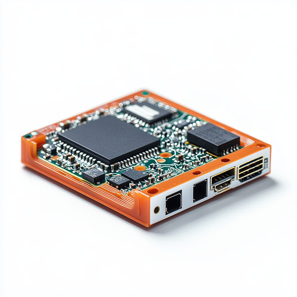
PCBA
When a PCB is surface-mounted or through-hole-mounted with components, we call this semi-finished product a PCBA. It can further assemble with other PCBAs and an enclosure to become a complete product or box-build we call it.
SMD
Surface mount device, it is an electronic component for SMT manufacturing. Compared with PTH components for PTH assembly, SMDs have a much smaller weight and size about 1/10 of a PTH component of the same function.
How Many Steps are in the SMT Process?
The SMT process involves several detailed steps, each essential for ensuring the quality and reliability of the final electronic product. Below is a comprehensive look at these steps:
Step 1: Components Incoming Inspection
Before the assembly begins, all components undergo an incoming inspection. This step is crucial to ensure that all parts meet the required specifications. It helps in identifying any defects or discrepancies in the components, which could affect the final product’s quality.
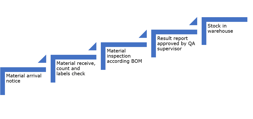
Step 2: PCB Quality Control
The next step is to inspect the PCB itself. This involves checking for any manufacturing defects, such as scratches, misalignments, or irregularities in the copper layers. Ensuring the PCB is flawless is vital because any defect can lead to failure in the final assembly.
Step 3: Stencil Preparation
Stencil preparation is critical for the accurate application of solder paste. The stencil must be aligned correctly with the PCB to ensure the solder paste is applied precisely to the pads where components will be placed. This accuracy is key to avoiding soldering defects.
Step 4: Solder Paste Applying
Solder paste is applied to the PCB through the stencil. The paste contains tiny balls of solder mixed with flux, and it’s applied to the areas where components will be soldered. Proper application of the solder paste is essential for creating reliable solder joints.
Step 5: SPI (Solder Paste Inspection)
After applying the solder paste, it’s inspected using SPI (Solder Paste Inspection) equipment. This step checks the volume, height, and position of the solder paste on the PCB. Any deviations from the ideal paste deposit can lead to defects, so this inspection helps ensure consistency and quality.
Step 6: Pick and Place Components
The pick and place machine automatically places components onto the PCB. Misplaced components can lead to electrical failures, so this step is critical for the overall success of the process.
Step 7: Reflow Soldering
Once the components are placed, the PCB is passed through a reflow oven. The heat in the oven melts the solder paste, creating a solid electrical connection between the components and the PCB. The reflow process must be carefully controlled to avoid overheating or insufficient soldering.
Step 8: AOI (Automated Optical Inspection)
After reflow soldering, the board undergoes AOI. This inspection process uses cameras to check for soldering defects, such as bridges, misaligned components, or insufficient solder. AOI helps catch defects early, reducing the chances of failures in the final product.
Step 9: X-RAY (Only for BGA or Fine-Pitch Components)
For boards with Ball Grid Array (BGA) or fine-pitch components, an X-ray inspection is performed. This step allows for the inspection of solder joints that are hidden beneath the components, ensuring that they are properly formed and free of defects.
Step 10: FAI (First Article Inspection)
The first board produced in a batch undergoes FAI, where it is thoroughly inspected to ensure that all processes and setups are correct. This step serves as a final check before full production begins, helping to confirm that everything is in order.
Step 11: Function Testing
The final step in the SMT process is function testing. This involves testing the completed PCB to ensure it functions as intended. Function testing is essential to verify that the board meets the required specifications and operates correctly in its intended application.
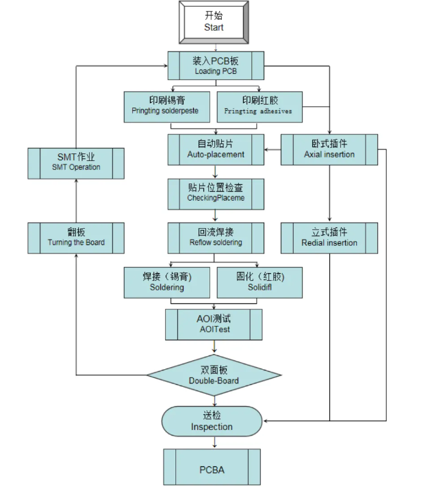
SMT Process Flow Chart
A flow chart is a visual representation of the SMT process, showing each step in sequence. This chart is essential for understanding how the process works and identifying potential areas for improvement. Here’s a basic flow chart of the SMT process:
How Do I Prepare for SMT?
Preparing for the SMT process requires careful planning and attention to detail. Here are some tips to help you get ready:
- Design for Manufacturability (DFM)
- Material selection
- Stencil
- Equipment calibration
- Quality control
- Training
EBest Circuit (Best Technology) – Your Turn-key PCB & PCBA Supplier
At EBest Circuit (Best Technology), we offer a range of value-added services, including IC programming, functional testing, conformal coating, thermal aging, and box-build assembly, ensuring you receive fully assembled and ready-to-use electronic products.
Additionally, you can reduce fabrication costs without compromising on function or quality. If needed, EBest Circuit (Best Technology) can source alternative components with equivalent functions and certifications to replace more expensive parts as well.
Tags: smt process, surface mount process