
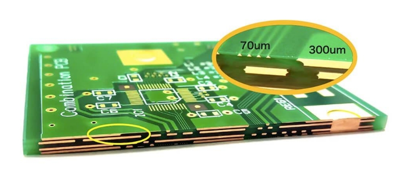
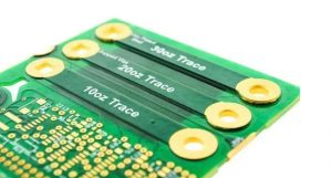
PCB copper thickness is generally divided into 1OZ (35um), 2OZ (70um), 3OZ (105um), of course, there are thicker ones. The copper thickness depends on what kind of board you are making. For example, 2OZ is enough for switching power supplies with high current, and 1OZ is enough for general signals.
Generally, double-sided boards are 1oz
Multi-layer boards are generally 1/2oz 1/3oz for the inner layer and 1oz 1/2oz 1/3oz for the outer layer
0.5 oz copper thickness About 0.685 mm.
1 ounce is about 1.37 mm, so 1.37÷2=0.685,
0.5 oz copper thickness in mm About 0.685 mm
1 oz copper thickness: This is the most common and basic copper thickness standard, also known as standard copper thickness. 1 oz copper thickness refers to the weight of 1 ounce (about 35.3 grams) of copper foil per square foot of board area, and the corresponding copper foil thickness is about 1.4 mils (0.035mm). This copper thickness is suitable for most common circuit board designs and applications.
2 oz copper thickness: 2 oz copper thickness refers to the weight of 2 ounces (about 70.6 grams) of copper foil per square foot of board area, and the corresponding copper foil thickness is about 2.8 mils (0.071mm). This copper thickness is suitable for some applications that require higher current carrying capacity, such as power electronic devices and high-power LEDs.
3 oz copper thickness: 3 oz copper thickness refers to the weight of 3 ounces (about 105.9 grams) of copper foil per square foot of board area, and the corresponding copper foil thickness is about 4.2 mils (0.107mm). This copper thickness is suitable for some special applications that require higher current carrying capacity, such as high-power amplifiers and high-power power supplies.
PCB copper foil thickness standard
- Common international PCB thicknesses are: 35um, 50um, and 70um.
- The copper foil (copper cladding) thickness of general single-sided and double-sided PCBs is about 35um (1.4mil), and the other specifications are 50um and 70um.
- The surface thickness of multilayer boards is generally 35um=1oz (1.4mil), and the inner layer is 17.5um (0.7mil).
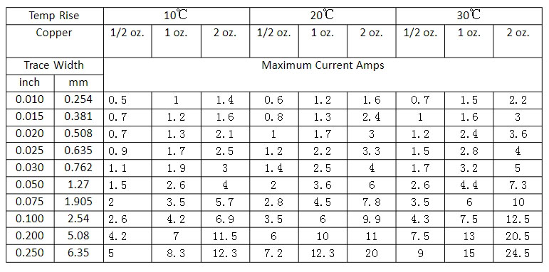
The relationship between the line width, copper thickness and current passing through the PCB board
1 foot = 12 inches
1 inch = 1000 mil
1mil = 25.4um
1mil = 1000uin mil is sometimes called inch
1um = 40uin (some companies call microinches “microinches”, which are actually microinches)
1OZ = 28.35 grams per square foot = 35 microns
PCB copper thickness current comparison table
Copper foil width Copper foil thickness
70um 50um 35um
2.50mm 6.00A 5.10A 4.50A
2.00mm 5.10A 4.30A 4.00A
1.50mm 4.20A 3.50A 3.20A
1.20mm 3.60A 3.00A 2.70A
1.00mm 3.20A 2.60A 2.30A
0.80mm 2.80A 2.40A 2.00A
0.60mm 2.30A 1.90A 1.60A
0.50mm 2.00A 1.70A 1.35A
0.40mm 1.70A 1.35A 1.10A
0.30mm 1.30A 1.10A 0.80A
0.20mm 0.90A 0.70A 0.55A
0.15mm 0.70A 0.50A 0.20A
PCB copper content
The copper content of PCB copper foil is generally 90% and 88%.
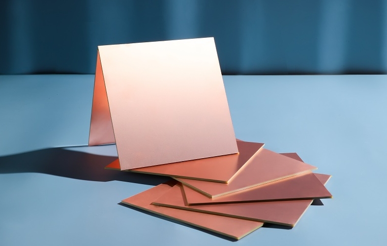
Copper foil is made of copper and a certain proportion of other metals. There are two common specifications of copper foil, namely 90% and 88% copper content. The size of these two specifications of copper foil is 16*16cm, which is widely used in various occasions where copper foil is needed, including PCB manufacturing. In PCB manufacturing, copper foil is the basic material of the circuit board, and its thickness and copper content have an important influence on the electrical performance and durability of the circuit board. The thickness of copper foil is usually expressed in OZ (ounces). The standard PCB copper thickness range is 1/4OZ-6OZ. The specific thickness includes 1OZ, 2OZ, 3OZ, 4OZ, 5OZ, 6OZ, which correspond to different copper thickness sizes, such as 35um, 70um, 105um, 140um, 175um, 210um. In practical applications, the commonly used copper thicknesses are 1OZ, 2OZ, 3OZ, 4OZ, etc. These copper thicknesses can meet the needs of most electronic products.
Why is the copper foil on the surface of PCB copper+plating?
The copper foil on the surface of the PCB adopts the copper+plating method, mainly because this treatment method can provide better conductivity and protection circuit. Copper foil is the conductor of PCB, and its basic material is copper, while plating (plating) is a layer of metal added on the basis of copper foil by electroplating or other methods, usually tin, gold or other alloys, to provide additional protection and enhance electrical performance. The reasons and advantages of this treatment method are as follows:
- Conductivity: Copper has good conductivity and is an ideal medium for the flow of electrons. In PCB, copper foil is used as a conductive layer to connect various electronic components and ensure smooth transmission of current.
- Protective circuit: By adding plating, such as tin or gold, to the copper foil, additional protection can be provided to prevent the copper foil from being oxidized or corroded, thereby protecting the long-term stability and reliability of the circuit board.
- Enhanced electrical performance: Plating not only prevents copper foil from being oxidized, but also enhances electrical performance by selecting appropriate plating materials, such as using gold plating to improve the corrosion resistance and conductivity of the circuit board.
- Cost considerations: Although gold is an expensive metal, the use of gold plating in certain key signal lines or high-density interconnection areas can significantly improve the performance and reliability of the circuit board, especially in reducing signal loss and interference in high-frequency signal transmission.
You may also like


Tags: copper thickness, PCB