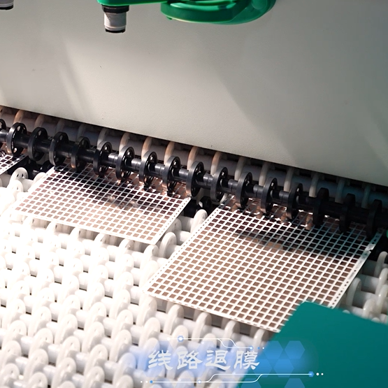
Ceramic PCB etching is a process that removes copper from a ceramic PCB by chemical methods to leave only the required copper traces on the board. This allows the creation of conductive paths between the components on the ceramic PCB that make up the circuit. Etching is a key step in ceramic PCB manufacturing, which can make ceramic PCB manufacturing efficient and up to standard.
During the ceramic PCB etching process, the chemical etchant solution dissolves the unwanted copper on the ceramic PCB laminate, while the resist (usually a polymer film) protects the copper traces from being etched away. After the etching is completed, only the desired copper circuit pattern remains on the ceramic PCB.
What are the reasons for uneven etching?
The reasons for uneven etching mainly include insufficient etching solution concentration, high or low temperature, long or short time, incomplete film stripping on the substrate surface, residual film, uneven thickness of copper plating on the board surface when copper is plated on the entire board, etc.
Uneven etching is one of the problems often encountered in the ceramic PCB etching process, and its reasons are diverse and complex. First of all, the problem of etching solution is an important factor leading to uneven etching. If the concentration of the etching solution is insufficient, or the temperature is too high or too low, or the etching time is too long or too short, uneven etching may occur. These problems can be solved by adjusting the concentration of the etching solution, controlling the etching temperature within an appropriate range, and ensuring that the etching time is within a reasonable range.
In addition, improper surface treatment of the substrate is also one of the reasons for uneven etching. If the film on the substrate surface is not completely removed, there is residual film, or the thickness of the copper plating layer on the board surface is uneven when the copper is plated on the entire board, the uniformity of etching will be affected. Similarly, if the ink is stained on the transmission roller of the etching machine when the board surface is corrected or repaired with ink, uneven etching may also occur.
How to avoid uneven etching?
Optimize the design of the etching tank: ensure the uniform distribution of the etching solution in the etching tank, design a reasonable liquid flow path, and improve the fluidity and uniformity of the etching solution.
Control the etching time: Reasonably control the etching time, avoid too long or too short etching time, and ensure uniform etching.
Stabilize the concentration of etching solution: Regularly monitor and adjust the concentration of etching solution to ensure the chemical composition of etching solution is stable.
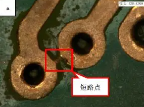
How does the residue problem affect the etching quality?
Impact on etching uniformity: The presence of residues and impurities may have a serious impact on the success of the etching process, especially at the micro-nano scale, these residues and impurities may affect the uniformity of etching, resulting in a decrease in etching quality.
Affect the uniformity and stability of etching solution: Residues and impurities may affect the uniformity and stability of etching solution, thereby affecting the quality of etching process. Factors such as etching solution concentration, pressure strength, temperature, speed and environment are all key factors affecting etching quality, and the presence of residues may interfere with the normal function of these factors, resulting in a decrease in etching quality.
Affect the etching performance and quality of metal materials: The type and microstructure of metal materials have a significant impact on the etching process and quality. Alloy materials containing different elements will form micro-corrosion cells during the corrosion process, affecting the dissolution rate and uniformity of the metal corrosion process. The presence of residues may aggravate this effect, resulting in a decrease in etching quality.
Requires additional cleaning and processing steps: In order to remove the residue, additional cleaning and processing steps may be required, which may increase production costs and time. In addition, if the residue is difficult to remove or detect, it may also affect the quality and performance of the final product.
How to avoid the problem of residue?
Use pure etching solution: Select high-purity etching solution to ensure the purity and chemical activity of the etching solution.
Increase cleaning steps: Use a multi-step cleaning process to completely remove the etching solution and etching products to ensure that the surface is clean and residue-free.
Optimize process control: Strictly control parameters such as temperature, time, and concentration during the etching process to ensure stable etching effects.
What problems will over-etching cause?
Over-etching of ceramic PCBs will cause a series of problems, including excessive circuit etching, local corrosion, galvanic corrosion, etc.
Excessive circuit etching: When the circuit design is too detailed and the copper foil used is thick, it may cause excessive circuit etching, resulting in abnormal copper foil peeling strength, thus affecting the normal function of the circuit.
Local corrosion: includes filiform corrosion, crevice corrosion, and pitting corrosion. These types of corrosion are usually caused by chemical reactions between oxygen, moisture in the air and copper, or by corrosion in these crevices due to residual materials, hardware, or areas under components on the PCB.
Galvanic corrosion: When two different metals are coupled in a corrosive electrolyte, galvanic corrosion, also known as bimetallic corrosion, occurs.
In summary, excessive etching of ceramic PCBs may not only cause abnormal circuit function, but also cause a variety of corrosion problems, thus affecting the overall performance and life of the circuit board.
How to avoid excessive etching?
Reasonably control the etching time: According to the specific process requirements, reasonably control the etching time to ensure that the etching depth is moderate.
Adjust the etching solution concentration: According to the etching requirements, adjust the etching solution concentration to control the etching rate.
Optimize process parameters: During the etching process, strictly control process parameters such as temperature and pressure to avoid excessive etching.
How does graphic distortion affect the etching effect?
The main causes of graphic distortion include poor photoresist graphics, uneven distribution of etching solution, and improper etching process control.
Poor photoresist pattern: During the photolithography process, the photoresist pattern is unclear and uneven, which will cause the circuit pattern to be distorted after etching.
Uneven distribution of etching liquid: The uneven distribution of etching liquid in the etching tank will lead to different etching rates in different areas, resulting in inconsistent line width and shape, and pattern distortion.
Improper control of etching process: Improper control of process parameters such as temperature, time, and concentration during etching will lead to unstable etching rate and pattern distortion.
How to avoid image distortion?
Improve the quality of photoresist patterns: Use high-quality photoresist to ensure clear and uniform photolithography patterns and improve pattern accuracy.
Optimize etching tank design: Design a reasonable etching tank to ensure uniform distribution of etching liquid in the tank and reduce pattern distortion.
Strictly control process parameters: During the etching process, strictly control process parameters such as temperature, time, and concentration to reduce pattern distortion.
There are many common problems in the etching process of ceramic PCBs. These problems can be effectively solved by reasonably controlling the etching time, adjusting the etching liquid concentration, and using high-precision equipment. As a professional ceramic circuit board manufacturer, BEST Technology has 18 years of experience in ceramic PCB production. It can provide high-quality products and comprehensive technical support to ensure the success of the project and the reliable operation of the equipment.