
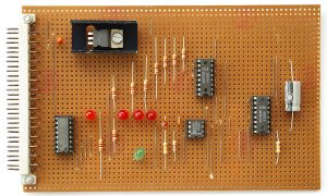
Copper can be said to be an indispensable element in printed circuit boards. In printed circuit boards, copper is used as a conductive line to connect electronic components and realize the function of the circuit. Compared with other conductive materials, copper has a lower resistance, which can reduce the loss of electric energy and improve the efficiency of electronic equipment.
What are copper printed circuit boards?
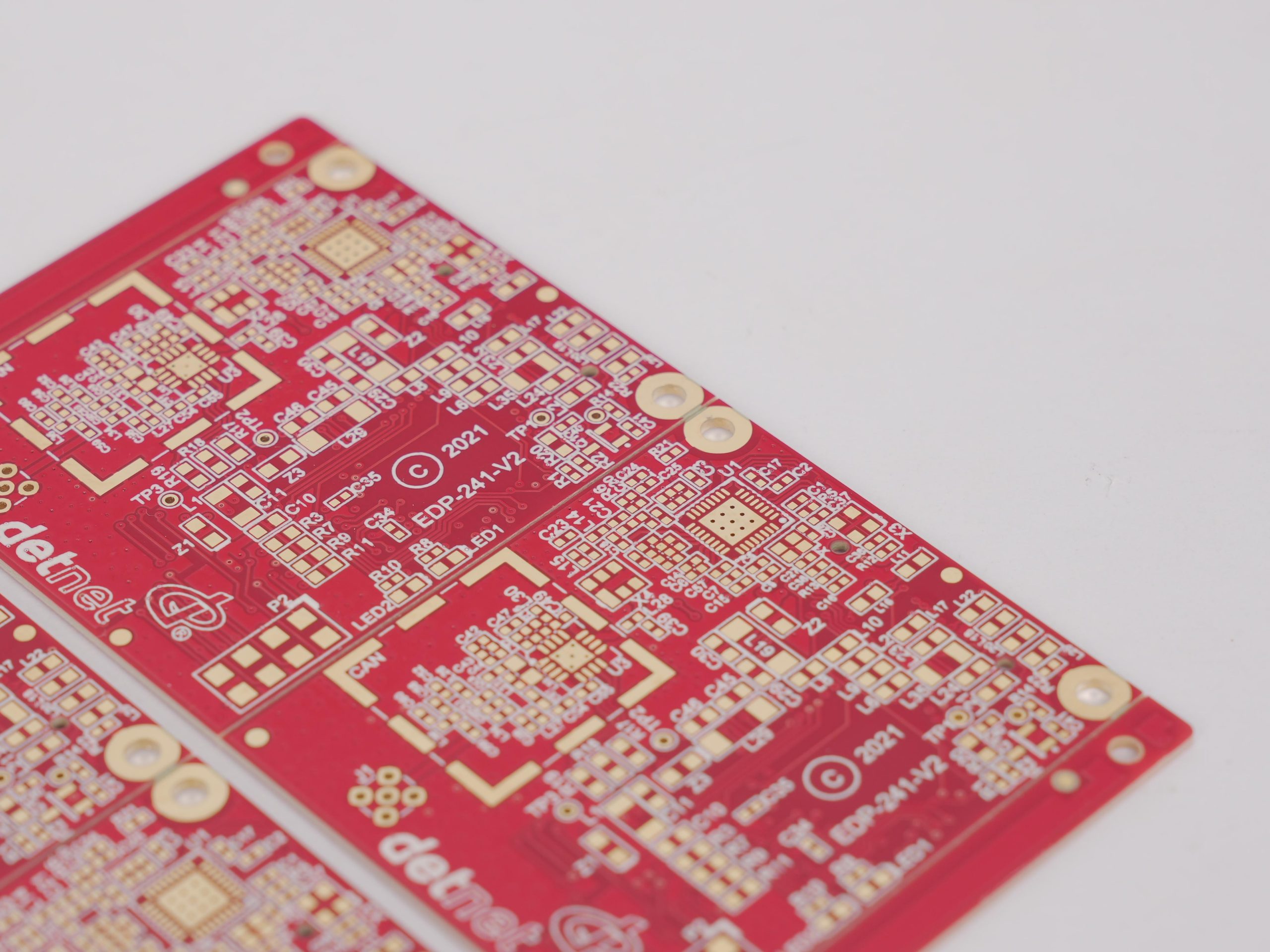
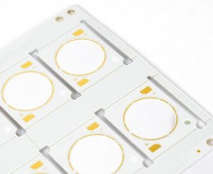
Copper printed circuit board (Copper PCB) is a printed circuit board with copper as the main conductive material. It is a circuit board with copper conductive paths formed on an insulating substrate through processes such as etching or electroplating. Its main function is to provide physical support and electrical connections for electronic components.
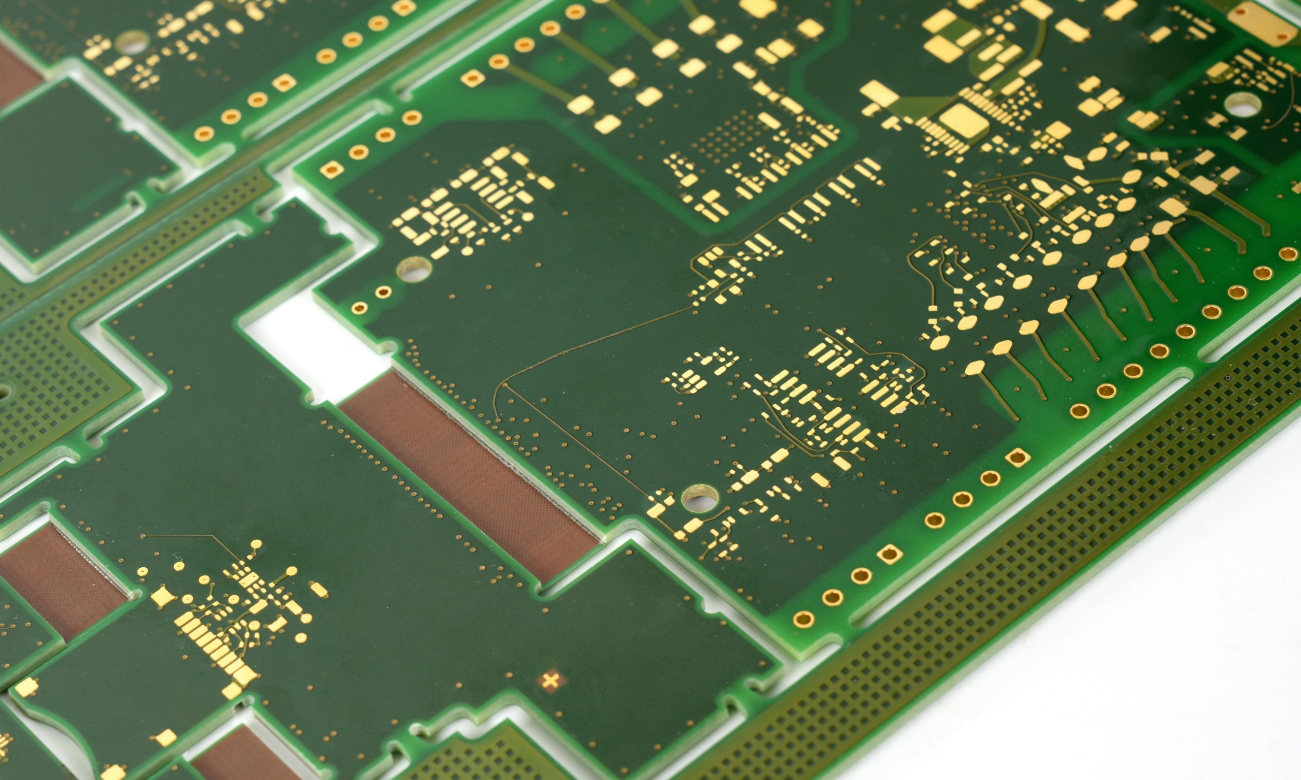
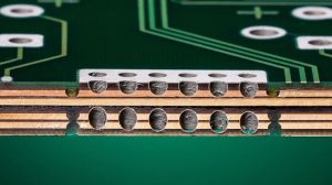
The structure of copper printed circuit boards usually includes insulating substrates, copper foil and surface treatment layers. Copper has excellent electrical conductivity and can efficiently transmit current. At the same time, its thermal conductivity is good, which helps to dissipate heat. Copper is easy to weld and suitable for the installation of electronic components. It has certain strength and toughness and can withstand certain mechanical stress.
In the manufacturing process, the production of copper printed circuit boards includes design and layout, inner layer production, lamination, drilling, copper plating, outer layer production, etching and surface treatment.
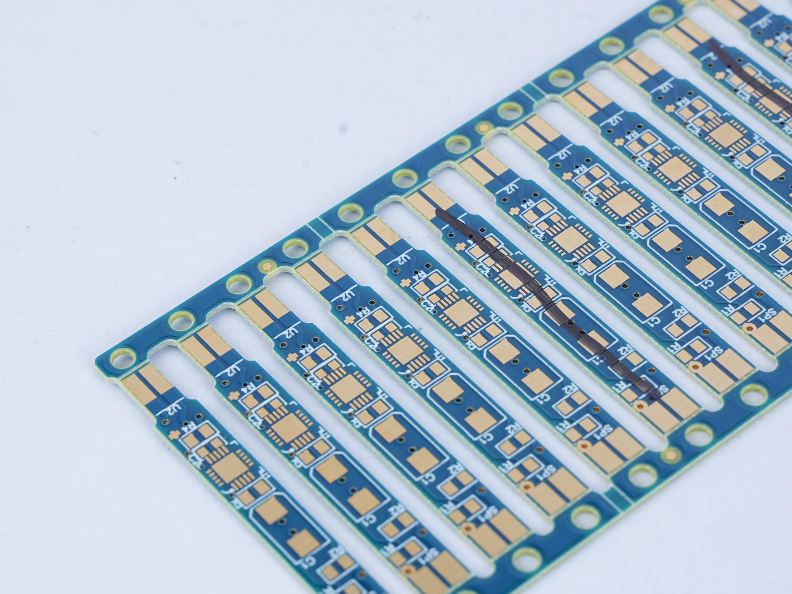
Copper printed circuit boards are widely used, including single-layer and multi-layer PCBs, high-current PCBs, flexible PCBs and thick copper PCBs.
Single-layer and multi-layer PCBs are suitable for simple electronic devices and complex multi-layer circuits; high-current PCBs are used for applications that require large current transmission; flexible PCBs are used for applications that require bending and folding; thick copper PCBs are used in scenarios with high power and high heat dissipation requirements.
Why is copper used in printed circuit boards?
The main reason for using copper in printed circuit boards is that copper has good conductivity, which can greatly improve the conductivity of the circuit board and ensure that the connection between various components is more stable and reliable.
In addition, copper foil itself has high mechanical strength and stability, which can effectively prevent the printed circuit board from being damaged or deformed by the external environment.
In terms of high-frequency signal transmission, copper plating can effectively improve the conductor characteristics and impedance matching characteristics of the circuit board, protect the circuit board from oxidation or corrosion, thereby extending the service life of the circuit board and ensuring its stability and reliability.
Copper plating can reduce the voltage drop in the circuit, thereby improving the efficiency of power supply. In addition, copper plating can also enhance the mechanical strength of the PCB, so that it will not deform as much as possible during the welding process, improve the yield rate in the production process, and reduce circuit failures caused by deformation.
However, copper plating also has its disadvantages. For example, when soldering or repairing PCB samples, it may cause difficulty in replacing devices due to excessive heat dissipation, especially in the case of large devices. In addition, in RF circuits, copper plating may cause impedance mutation of the antenna, seriously affecting signal transmission.
How thick is the copper on a printed circuit board?
The thickness of copper foil on a printed circuit board is usually between 18μm and 70μm, but the specific thickness depends on the purpose of the circuit board, the voltage and current of the signal.
The most commonly used copper foil thickness is 35μm, because the copper foil thickness of 35μm is suitable for most application scenarios. However, for applications that need to carry higher power or higher current, such as high-power LED lights, power supply circuits, etc., 2OZ (about 70μm) or thicker copper foil may be selected to ensure the performance of the circuit board and the reliability and stability of electronic products.
In addition, the copper thickness of the circuit board is also affected by the thickness of its substrate. For example, the composite copper foil thickness on a substrate less than 1mm thick is about 18μm, while a copper foil thickness of 55μm may be used on a substrate greater than 5mm.
How do you choose PCB copper thickness?
When choosing PCB copper thickness, you need to consider multiple factors to ensure the performance, cost and production feasibility of the circuit board.
- Application scenarios of circuit boards: For applications that need to carry high power or high current, you may need to choose thicker copper foil to ensure the stability and reliability of the circuit board. For general signal transmission, 1oz copper thickness is usually sufficient.
- Number of layers and design of circuit boards: The inner layer of multilayer boards generally uses 1/2oz and 1/3oz copper thickness, while the outer layer uses 1oz or 1/2oz copper thickness.
- Cost and process requirements: The thicker the copper foil, the higher the production cost. Therefore, it is necessary to consider cost factors while ensuring performance.
- Special requirements: In some special application scenarios, such as when the circuit board needs to dissipate heat, copper foil with higher thermal conductivity should be selected to enhance the heat dissipation capacity of the circuit board.
What is the difference between 1 oz and 2 oz copper PCB?
The main difference between 1 oz and 2 oz copper PCB lies in the thickness of the copper foil and the current load it can withstand.
- Copper foil thickness: 1 oz copper thickness refers to 1 ounce of copper per square foot on the circuit board, while 2 oz copper thickness refers to 2 ounces of copper per square foot.
- Application scenario: 1 oz copper thickness PCB is the most common standard and is suitable for most application scenarios. 2 oz copper thickness is suitable for application scenarios that need to carry higher power or higher current.
- Electrical performance and heat dissipation performance: In theory, thicker copper foil can directly reduce the ground resistance by half, and the number of joules of heat generated per unit time during operation will also be reduced accordingly. At the same time, it can more effectively shield the electromagnetic interference between components and wires.
How thick is the copper on a 1 ounce copper PCB?
The copper thickness of 1 ounce copper on a PCB is about 35 microns.
In PCB design and processing, the copper thickness is often expressed in ounces (oz) as a unit. Specifically, the thickness of 1 ounce of copper is about 35 microns, which is equivalent to 1.4 mils. Although this method of expression uses the weight unit ounce, it actually indirectly expresses the average thickness of the copper foil through the weight per unit area.
In the PCB industry, ounces are not only a unit of weight, but also used to express the thickness of copper foil, where 1oz means the thickness of 1 ounce of copper evenly laid on an area of 1 square foot. This method of expression is very common in the fields of electronic engineering and circuit board manufacturing to ensure that the conductivity and current carrying capacity of the circuit board meet the design requirements.
Which metals Cannot be used in printed circuit boards?
In the production of printed circuit boards, some metals are usually not used.
First of all, iron has poor conductivity and cannot meet the requirements of printed circuit boards for good conductive materials. Moreover, iron is easy to rust, which will affect the appearance of the circuit board and may also cause circuit short circuits or poor contact.
Lead is also not suitable for printed circuit boards. On the one hand, lead is a toxic heavy metal. With the improvement of environmental protection requirements, the use of lead-containing materials in the electronics industry is limited, and lead-containing solder in printed circuit boards has gradually been replaced by lead-free solder. On the other hand, lead has poor mechanical properties, low hardness and easy deformation, which may deform or damage the circuit board during manufacturing and use.
Mercury cannot be used in printed circuit boards. Mercury is extremely toxic and has serious harm to the human nervous system, immune system, etc. At the same time, mercury is liquid and volatile at room temperature, difficult to control, easy to cause leakage and pollution, and its conductivity is not ideal.
Although gold has advantages such as good conductivity, corrosion resistance and oxidation resistance, its cost is too high and it is not suitable for large-scale application in printed circuit boards. In addition, gold has low hardness and is easily scratched or worn, affecting the performance and reliability of the circuit board.
What is the major disadvantage of printed circuit boards?
The major disadvantages of printed circuit boards include disposable boards, environmental impact of etching, and compatibility issues.
- Disposable boards: Printed circuit boards are designed with one-time use in mind, which means that if the circuit board needs to be modified after printing, it will not be possible and a new board needs to be created from scratch.
- Environmental impact of etching: The chemicals used in the etching process have a negative impact on the environment. Although the etching process is very effective for circuit board production, it is not environmentally friendly.
- Compatibility issues: Before starting to make a circuit board, you need to determine the device you are designing for, which increases the complexity and potential risks of the design.
These shortcomings limit the use of printed circuit boards in some applications to a certain extent, especially in scenarios that require high customization or frequent modifications.
In short, copper printed circuit boards occupy an irreplaceable position in the electronics field with their excellent performance. From consumer electronics to communications, automotive electronics, and industrial control, it can be seen everywhere. Copper’s high electrical conductivity, good thermal conductivity, and strong machinability make it a key link connecting the electronic world.
You may also like


Tags: copper, copper thickness, PCB