
In the field of electronics, ceramic circuit boards are quietly opening a new revolution with their unique charm and excellent performance. Ceramic circuit boards are gradually becoming the focus of the electronics industry, leading the industry to a more efficient, stable and advanced technological era.
What is a ceramic pcb board?
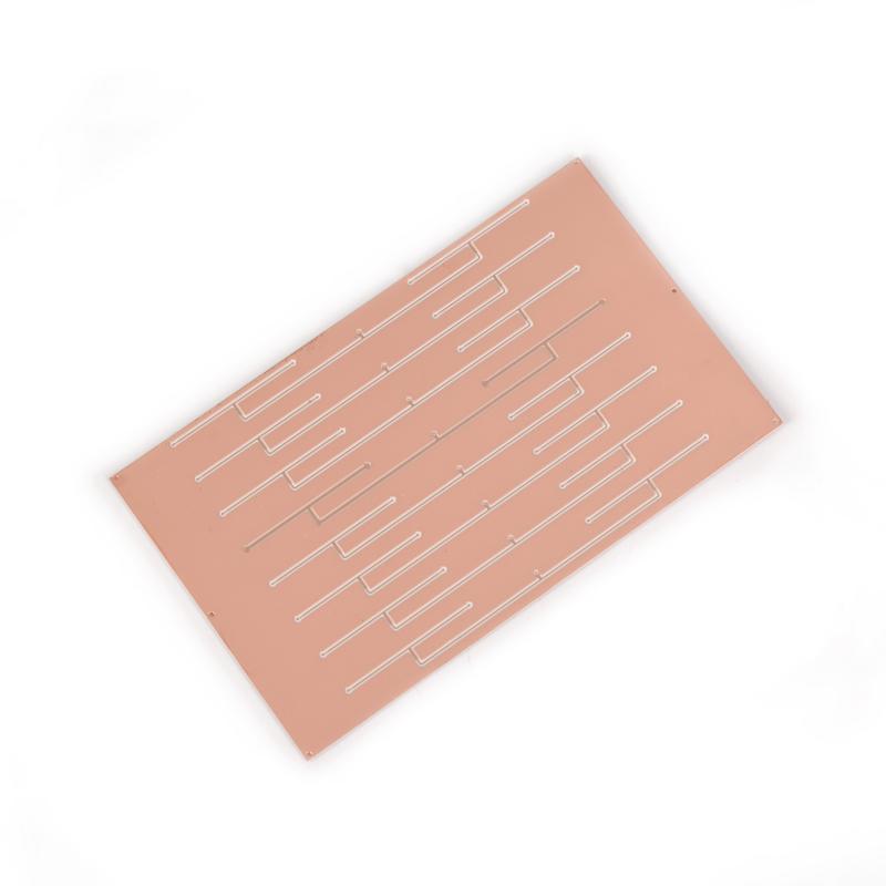
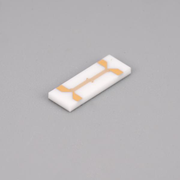
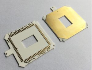
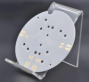
ceramic pcb board, also known as ceramic printed circuit board, is a printed circuit board that uses ceramic as a substrate instead of traditional fiberglass or epoxy resin. Compared with traditional substrates, ceramic materials have a variety of advantages, making them ideal for high-performance electronic applications.
What are the different types of ceramic PCB?
There are several types of ceramic materials commonly used in PCB boards, including aluminum oxide (Al₂O₃), aluminum nitride (AlN), and beryllium oxide (BeO). Each material has its own unique properties and advantages.
1. Alumina ceramic pcb board
Alumina is the most widely used ceramic material in PCB boards. It has excellent electrical insulation, high thermal conductivity and good mechanical strength. Alumina ceramic pcb boards are suitable for a wide range of applications, including power electronics, LED lighting and automotive electronics.
2. Aluminum Nitride ceramic pcb board
Aluminum nitride is a high-performance ceramic material with extremely high thermal conductivity. This makes it ideal for applications where heat dissipation is a key factor, such as high-power LEDs, power modules, and RF/microwave equipment.
3. Beryllium Oxide ceramic pcb board
Beryllium oxide is a highly toxic material, but it has excellent thermal conductivity and electrical insulation. Due to its toxicity, beryllium oxide ceramic pcb boards are only used in special applications where other materials cannot meet the performance requirements.
What is the high temperature ceramic PCB?
High temperature ceramic PCB is a special ceramic circuit board designed for high temperature environments, commonly known as high temperature co-fired ceramic (HTCC) circuits. This circuit board is made by mixing adhesives, lubricants, solvents, plasticizers, and aluminum oxide to make raw ceramics, and then forming circuits.
The main feature of high temperature ceramic PCBs is their high temperature resistance, which allows them to work stably under extreme temperature conditions, making them ideal for applications that require high reliability and long-term stability.
In addition, during the manufacturing process of high-temperature ceramic PCB, the copper foil and the ceramic substrate are bonded together. This bonding method not only has strong bonding strength, but also the copper foil will not fall off, thus ensuring the performance stability in harsh environments such as high temperature and high humidity.
The materials of high-temperature ceramic PCB usually include ceramic materials such as aluminum oxide (Al2O3), beryllium oxide (BeO), aluminum nitride (AlN), silicon carbide (SiC) and boron nitride (BN). These materials are not only very effective in conducting heat, but also good electrical insulators, making high-temperature ceramic PCBs perform well in applications that require high thermal conductivity and excellent electrical properties.
In general, high-temperature ceramic PCB is a high-performance, high-reliability circuit board, especially suitable for applications that require high thermal conductivity, excellent electrical properties, and stable operation in harsh environments, such as aerospace, military electronics, etc.
What are the manufacturing processes involved in ceramic pcb boards?
The manufacturing process of ceramic pcb boards is more complicated than that of traditional PCB boards. It generally involves the following steps:
1. Substrate preparation
Ceramic substrates are prepared by sintering ceramic powder at high temperatures. The sintered substrate is then polished and cleaned to ensure a smooth surface for subsequent steps.
2. Circuit pattern formation
Circuit patterns are formed on ceramic substrates using various methods, such as screen printing, photolithography, or laser ablation. In screen printing, a conductive paste is printed onto the substrate to form a circuit pattern. Photolithography involves the use of a photomask and photoresist to create a circuit pattern. Laser ablation uses a laser to remove unwanted ceramic material to form a circuit pattern.
3. Metallization
After the circuit pattern is formed, the substrate is metallized to provide conductivity. This is usually done by sputtering or electroplating a thin layer of metal, such as copper or gold, onto the substrate.
4. Component mounting
Electronic components are then mounted onto the ceramic pcb board using surface mount technology (SMT) or through-hole technology (THT). SMT involves soldering components directly onto the surface of the PCB board, while THT involves inserting components into holes in the PCB board and soldering them to the bottom surface.
What are the advantages of ceramic pcb boards?
ceramic pcb boards have several advantages over traditional PCB boards, making them ideal for high-performance electronic applications. Some of the main advantages include:
- 1. High thermal conductivity: Ceramic materials have excellent thermal conductivity, which allows for efficient heat dissipation.
- 2. High electrical insulation: Ceramic materials have high electrical insulation, which reduces the risk of electrical short circuits and improves the reliability of electronic devices.
- 3. Good mechanical strength: Ceramic materials have good mechanical strength, making them resistant to vibration and shock.
- 4. Small size and light weight: ceramic pcb boards can be made very thin and lightweight, making them ideal for portable electronic devices.
- 5. High-frequency performance: Ceramic materials have low dielectric losses and high frequency stability, making them suitable for high-frequency applications such as RF/microwave equipment.
What is a ceramic PCB used for?
Ceramic PCBs have a wide range of applications, including:
- 1. Power Electronics: Ceramic PCBs are widely used in power electronics applications such as power modules, inverters, and converters. The high thermal conductivity and electrical insulation of ceramic materials make them ideal for handling high power levels.

- 2. LED Lighting: Ceramic PCBs are used in LED lighting applications due to their excellent heat dissipation properties. The high thermal conductivity of ceramic materials helps to extend the life of LEDs by reducing operating temperatures.
- 3. Automotive Electronics: Ceramic PCBs are used in automotive electronics applications such as engine control units, power steering systems, and airbag controllers. The high mechanical strength and reliability of ceramic materials make them suitable for use in harsh automotive environments.
- 4. Aerospace and Defense: Ceramic PCBs are used in aerospace and defense applications due to their high performance and reliability. The small size and light weight of ceramic PCBs make them ideal for satellite and missile systems.
- 5. Medical Devices: Ceramic PCBs are used in medical devices such as pacemakers, defibrillators, and hearing aids. The high electrical insulation and biocompatibility of ceramic materials make them suitable for use in medical applications.
How is ceramic pcb board developing?
As the electronics industry continues to develop, there is a growing demand for high-performance PCB boards that can meet the growing requirements of advanced electronic devices. ceramic pcb boards are expected to play an important role in meeting this demand. Some future trends in ceramic pcb board technology include:
1. Increased use of high-performance ceramic materials
As the performance requirements of electronic devices continue to increase, there is a growing demand for high-performance ceramic materials such as aluminum nitride and silicon carbide. These materials have higher thermal conductivity and electrical insulation than traditional ceramic materials, making them ideal for next-generation electronic devices.
2. Passive component integration
In order to reduce the size and weight of electronic devices, there is a growing trend to integrate passive components such as resistors, capacitors, and inductors onto PCB boards.
3. 3D printing of ceramic pcb boards
3D printing technology is emerging as a promising method for manufacturing ceramic pcb boards. 3D printing can create complex geometries and structures that are difficult to achieve using traditional manufacturing methods.
4. Development of hybrid PCBs
Hybrid PCBs that combine ceramic and traditional substrates are being developed. Hybrid PCBs can use ceramic substrates for the power section and traditional fiberglass substrates for the signal section.
Ceramic PCBs are a revolutionary technology that offers several advantages over traditional PCBs. As the electronics industry continues to grow, ceramic PCBs are expected to play an increasingly important role in meeting the growing demand for advanced electronic devices.
You may also like


Tags: ceramic PCB, PCB, pcb design, PCBA