
What is Dam in PCB?
A dam PCB refers to the solder mask dam in a circuit board, a thin barrier that separates areas of exposed copper. The dam is created to prevent solder from flowing across areas where it isn’t wanted, especially during the assembly process. These barriers ensure precise and clean soldering, which is critical for the functionality of the circuit board.
What is a Solder Mask Dam?
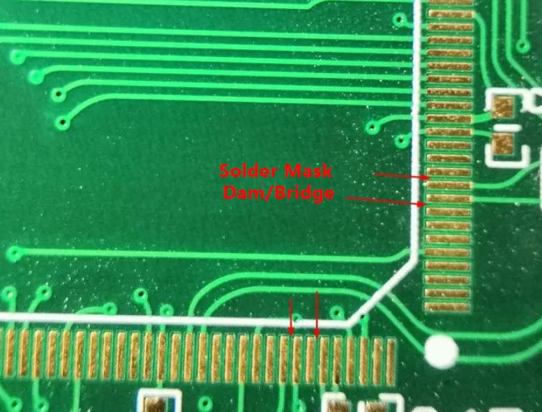
Solder mask dam, some engineers also call it solder resistance bridge. It is a narrow strip of solder mask material placed on the PCB between closely spaced pads or traces. It acts as a protective shield, ensuring that the solder sticks only to the pad used for the component and does not spread to adjacent areas.
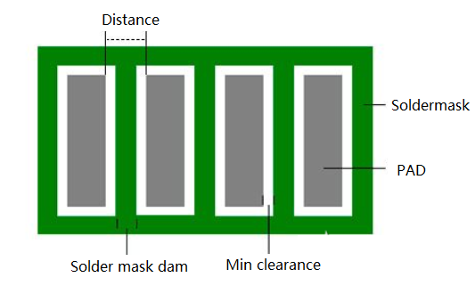
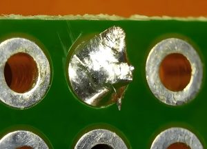
By introducing a small barrier, the solder mask dam ensures that solder joints are created only in the intended areas, thereby preventing electrical shorts and other types of damage that could lead to device malfunctions or failures. They safeguard copper traces and other metal features from oxidation, contamination, and other forms of damage. In the process of batch placement in the factory, the “isolation belt” of the solder resistance bridge can effectively avoid short circuit in the welding process of the SMD component pin, so as to ensure the normal operation of the electronic equipment. It can be said: without a proper solder stop dam, solder can flow uncontrollably, causing a short circuit or damaging other parts of the board.
Types of Solder Mask Dams
There are various types of solder mask dams, primarily depending on their width and the area of the PCB they protect. Each offering different advantages depending on the PCB design’s specific requirements. The main types include open, hatched, and round dams.
Open Solder Mask Dams
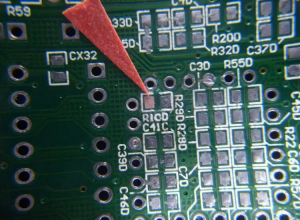
Open solder mask dams are the simplest and most commonly used type. They are created by leaving a small gap around each pad or through-hole, allowing solder to flow onto these areas without spreading to nearby conductive features. Here are their advantages:
- Simple to design and implement
- Suitable for most PCB designs
- Compatible with various soldering techniques
Hatched Solder Mask Dams
Hatched solder mask dams are similar to open dams but use a pattern of diagonal lines to create barriers around each pad or through-hole. These diagonal lines form small gaps in the solder mask, directing solder to the pad or through-hole while minimizing spreading.
It offers better protection against solder bridging compared to open solder mask dams and suitable for designs with closely spaced components or high-density PCBs.
Round Solder Mask Dams
Round solder mask dams use circular shapes to encircle each pad or through-hole. This circular barrier effectively prevents solder from flowing onto adjacent conductive features. Round solder mask dams provide the highest level of protection against solder bridging and damage. So it ideal for designs with fine-pitch components or high pin-count devices.
Role of Solder Mask Dams
The primary role of solder mask dams is to prevent solder from creating unintended connections between pads or traces. During the soldering process, when molten solder is applied to the PCB, it can sometimes spread beyond the desired area. A solder mask dam prevents this by creating a physical barrier.
- Prevention of solder bridges
Solder mask dams help prevent solder from flowing into unintended areas, reducing the risk of solder bridges and electrical shorts.
- Improve precision in soldering
By controlling where solder can flow, solder mask dams ensure that solder is applied only to the intended pads and through-holes.
- Protection against oxidation and contamination
Solder mask dams shield underlying copper traces from oxidation and contamination.
- Improved design flexibility
Solder mask dams allow for greater flexibility in PCB design by accommodating various component layouts and soldering techniques.
- Cleaner soldering process
By preventing solder from spreading to adjacent conductive features, solder mask dams contribute to a cleaner soldering process, resulting in fewer defects and a more polished final product.
How Solder Mask Dams Work?
The solder mask dam works by setting specific isolation strips on the printed circuit board (PCB) to prevent short circuits in the pins of the SMD components. The solder mask covers the part of the PCB that does not need to be welded, and the exposed part is the copper sheet that needs to be welded. The solder stop layer is set to follow the principle of negative output, that is, after the shape of the solder mask layer is mapped to the PCB, the exposed is actually copper, rather than the part with green oil. This design helps ensure the accuracy of the welding and the stability of the circuit.
In reflow welding process, solder mask layer is very important to control welding defects. The designer should minimize the spacing or air gap around the pad features to avoid the formation of tin Bridges. For closely spaced components, such as QFPS on four sides, the openings or Windows of the solder shield may require special consideration in order to facilitate control of the tin bridge between the element pins. In addition, the thickness of the solder mask is also an important factor, if the thickness is more than 0.04mm, it may affect the application of the solder paste.
Solder mask materials can be used by liquid wet process or dry film lamination. Dry film solder resistance materials are usually available in a thickness of 0.07-0.1mm and are suitable for some surface mount products, but are less recommended for close pitch applications. Liquid photoresist materials are often specified for surface mount applications due to their economy and accuracy.
What is the Minimum Solder Mask Dam?
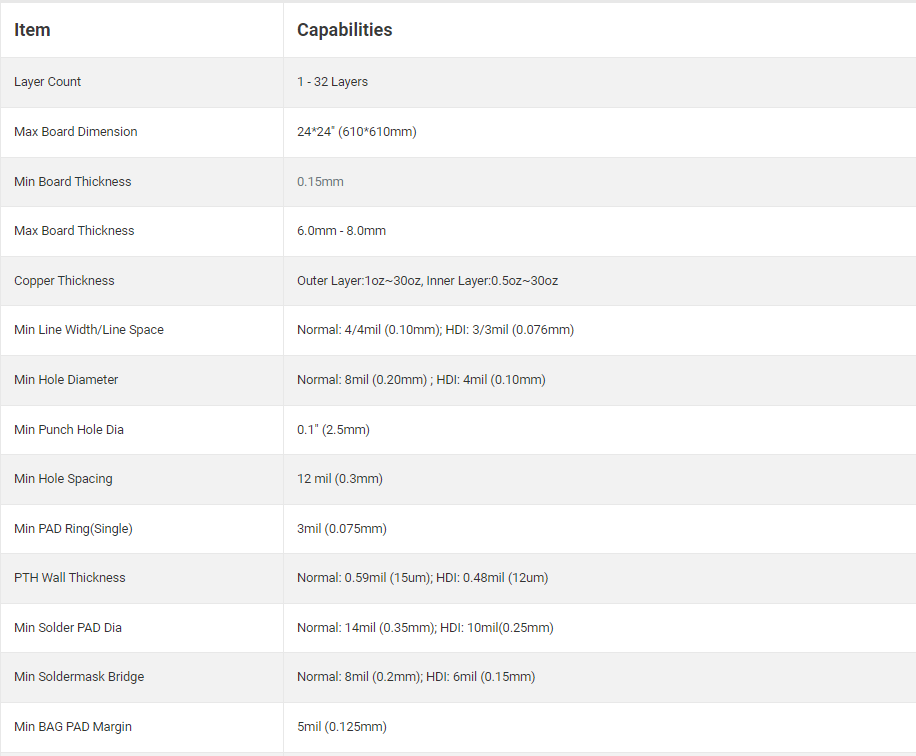
The minimum width of a solder mask dam depends on the design rules of the PCB manufacturer and the capabilities of the solder mask material. Typically, the minimum solder mask dam width ranges from 6 to 8 mils. In high-density designs, where components are packed closely together, achieving a consistent and effective solder mask dam at the minimum width can be challenging. Here is the PCB manufacturing capability in Best Technology of FR4 PCB:
How Thick Should Solder Mask Be in PCB?
The thickness of the solder mask plays a crucial role in its effectiveness. Standard solder mask thickness is usually between 15 to 25 microns. This thickness provides adequate protection against solder bridging while allowing the mask to withstand the heat and pressure of the soldering process. If the solder mask is too thin, it may not provide sufficient protection, leading to solder bleed. Conversely, if it’s too thick, it can cause misalignment issues during the assembly process.
How to Design a Solder Mask Dam?
Designing an effective solder mask dam requires careful planning and attention to detail. Here are key steps to follow when designing a solder mask dam:
1. Evaluate Component Density: Start by assessing the layout of your PCB. For high-density boards, you’ll need to design thinner dams that still provide sufficient protection.
2. Check Manufacturer’s Guidelines: Manufacturers have specific design rules for solder mask dams. It’s important to consult these guidelines to ensure your design meets the minimum and maximum dam widths allowed.
3. Optimize Pad and Trace Spacing: Ensure that there’s enough spacing between pads and traces to accommodate the solder mask dam. The spacing should be consistent to prevent solder bridges.
4. Simulate Solder Flow: Use simulation tools to visualize how the solder will flow during the assembly process. This helps identify areas where the solder mask dam may need to be adjusted for optimal performance.
5. Review Tolerance Requirements: PCB manufacturing involves tight tolerances. Make sure your solder mask dam design accounts for potential variations during fabrication.
Best Technology is a leading PCB manufacturer in Asia, we are certificated with ISO9001, IAFT16949, ISO13485 quality control systems to monitor our quality process. Get touch with us now to get your PCB instant quotes!
You may also like


Tags: pcb dam, solder mask dam, soldermask dam