
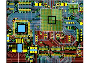
What is High Voltage PCB?
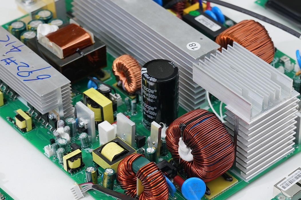
High voltage printed circuit boards (HV PCBs) are specialized boards designed to handle electrical voltages significantly higher than standard levels. These PCBs are used in industries like power distribution, telecommunications, and electric vehicles, where safe management of high voltage is critical. HV PCBs need to be carefully constructed using materials that can withstand electrical stress, heat, and prevent arcing between components. Their design also ensures that they meet strict safety standards, as high voltages can pose serious risks if not managed properly.
What is the High Voltage Warning on a PCB?
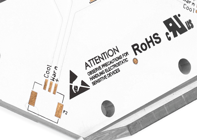
You may have seen a high voltage warning symbol on some PCBs. This is not just a cautionary mark; it’s a key safety feature. This warning typically comes in the form of a printed symbol, often a lightning bolt enclosed in a triangle, accompanied by a numerical value indicating the voltage present. These labels are essential for preventing accidents or injuries, as working with high voltage circuits without the proper knowledge or safety precautions can result in serious harm.
In addition to warning symbols, there might be specific color coding used on the board to indicate areas of high voltage. Some manufacturers use bright colors, like yellow or red, to highlight hazardous zones on the PCB. These visible indicators help ensure that anyone handling the PCB knows which areas to avoid or treat with extreme caution.
High voltage warnings also serve a legal function by complying with industry safety standards, such as those set by IPC (Institute for Interconnecting and Packaging Electronic Circuits). These standards mandate the inclusion of warning labels on PCBs to reduce the risk of electrocution, equipment damage, or unintended malfunctions.
In environments where multiple boards or systems are interconnected, high voltage warnings prevent confusion. Technicians can immediately identify which components or boards require extra care. By prominently displaying these warnings, PCBs protect users from accidental contact with potentially lethal voltages.
What is the Best Material for High Voltage PCBs?
Choosing the best material for a high voltage PCB involves selecting one that can withstand electrical stress and provide effective insulation. Standard PCBs typically use FR4, which is a glass-reinforced epoxy laminate material. While FR4 is suitable for low to medium voltage applications, it may not be the ideal choice for high voltage circuits, where electrical insulation and heat resistance are critical.
- Polyimide
For high voltage PCBs, materials like polyimide and ceramic are considered superior options:
Polyimide: This material offers excellent thermal stability, making it highly resistant to high temperatures generated by high voltage circuits. Polyimide is also flexible, allowing for its use in flexible PCB designs while maintaining strong electrical insulation properties. It’s an ideal choice for high voltage applications where heat and electrical performance are both concerns.
- Ceramics
Ceramic-based materials are preferred for extreme high voltage applications due to their outstanding dielectric properties. Ceramics can handle higher voltages than polyimide or FR4 and offer better thermal management. They are often used in power electronics, aerospace, and medical equipment where high voltage and reliability are paramount. Ceramic substrates provide a lower coefficient of thermal expansion, making them more durable under electrical stress.
- PTFE (Polytetrafluoroethylene)
PTFE-based laminates, such as those branded as Teflon, are also used in high voltage PCBs. PTFE provides excellent dielectric strength, low dissipation factors, and is highly resistant to temperature fluctuations. This material is useful for RF (radio frequency) applications as well, where both high voltage and high frequencies are factors.
What is the Clearance for High Voltage PCB?
Clearance refers to the physical distance between two conductive elements on a PCB that are not electrically connected. In high voltage PCBs, clearance is a critical factor to prevent electrical arcing or discharge between components. The clearance depends on the operating voltage and the environment the board is exposed to. Typically, the higher the voltage, the more clearance is required. For example, a PCB handling 1,000 volts will need significantly more space between traces than one dealing with 100 volts.
Clearance values are not arbitrary; they are determined by international safety standards like IPC-2221. The clearance required depends on the operating voltage, with higher voltages demanding larger gaps between conductive traces or components. As a general guideline:
- For voltages up to 100V, a clearance of about 0.1mm is sufficient.
- Between 100V and 1000V, the clearance typically ranges from 0.6mm to 5mm.
- For very high voltages above 1000V, clearances of 5mm or more might be necessary.
These values can also be influenced by environmental conditions such as humidity, contamination, or the presence of conductive particles. Higher humidity levels, for example, can reduce air’s insulating capacity, increasing the risk of electrical arcing. To account for these factors, many designers apply a safety margin to the clearance requirements, ensuring the PCB operates reliably even in less-than-ideal conditions.
Clearance vs Creepage in High Voltage Circuits
In high voltage circuits, both clearance and creepage are critical to maintaining electrical isolation and preventing breakdowns. Though often confused, these two terms refer to distinct aspects of circuit design:
- Clearance
As discussed earlier, clearance is the shortest distance between two conductive points through the air. It is essential in preventing electrical arcing between parts of a circuit, especially in high voltage PCBs. The higher the operating voltage, the greater the required clearance to ensure safety and functionality.
- Creepage
Creepage, on the other hand, refers to the distance along the surface of an insulating material between two conductive elements. This measurement is especially important in high voltage environments because surface contamination (like dust, moisture, or debris) can reduce the effective distance, allowing unintended current flow across the board’s surface.
While clearance deals with the air gap, creepage accounts for the surface path. In high voltage designs, both need to be carefully calculated, as inadequate distances can lead to unintended arcing, short circuits, or the degradation of the PCB over time.
Several factors influence creepage requirements:
1. Voltage Level: Higher voltages require longer creepage distances to prevent leakage currents.
2. Pollution Degree: The environmental conditions in which the PCB will operate affect creepage. In cleaner environments (like medical devices or sealed electronics), the required creepage can be lower. However, in industrial or outdoor applications, where dirt and moisture are present, larger creepage distances are needed.
3. Material: The type of insulation material used on the PCB affects creepage. Different materials have varying levels of resistance to surface conductivity, so choosing a high-quality insulating material can reduce creepage risk.
Designers must account for both clearance and creepage when building high voltage PCBs. Ignoring these factors can lead to dangerous conditions, equipment failure, or accidents. Following guidelines like those outlined by IPC-2221 ensures that both clearance and creepage distances are adequate, protecting the PCB from high voltage hazards.
How Much Voltage Can a PCB Handle?
The amount of voltage a PCB can handle depends on several factors, including the materials used, the layout design, and the operating environment. Typically, standard PCBs can handle voltages up to around 100 volts without special considerations. However, high voltage PCBs are designed to safely manage thousands of volts. For instance, some power distribution PCBs can handle upwards of 10,000 volts, provided they’re made with appropriate materials and have sufficient clearance and creepage.
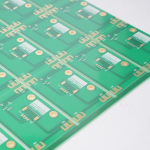
What is Solder Mask for High Voltage PCBs?
The solder mask is the protective layer applied over the copper traces on a PCB. For high voltage PCBs, the solder mask plays an important role in preventing short circuits and electrical arcing. A thicker or more specialized solder mask may be used for high voltage boards to provide extra insulation. It also helps prevent corrosion and protects the copper from environmental damage, extending the PCB’s lifespan in harsh conditions.
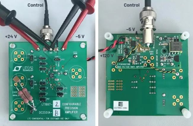
How Do You Check PCB Voltage?
Checking the voltage of a PCB requires careful handling, especially in high voltage applications. To check the voltage of the PCB (printed circuit board), you can do it in the following ways:
1. Use a voltmeter to measure directly
This is the most direct and accurate method. First, ensure that the circuit is in the off state, and select the appropriate voltmeter, according to the voltage range of the PCB select the appropriate voltmeter. If the PCB voltage is in the low voltage range, you can choose a digital multimeter for measurement; If the voltage is high, select a high voltage meter. Connect the positive and negative terminals of the voltmeter to the positive and negative terminals of the PCB respectively to ensure that the range of the voltmeter is set correctly to prevent damage to the voltmeter or PCB. Read the reading on the voltmeter, which is the PCB voltage 12.
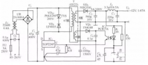
2. Check the circuit diagram
The circuit diagram is an important tool to understand the PCB voltage. If you have a circuit diagram at hand, you can determine the voltage of the PCB by consulting the circuit diagram. The circuit diagram will mark the voltage of each part, such as power input, output, etc. .
3. Check product manual
The product manual usually describes the PCB parameters in detail, including the voltage. By referring to the product manual, you can get accurate voltage information .
4. Find the circuit sign
Generally, many PCBs will mark the voltage value, especially commercial finished PCBs. These identifiers are usually printed on the surface of the board, or near the connector. Look for printed voltage labels, which usually end in “V”, such as “5V”, “12V”, etc .
Warm tips: Observe safety when measuring, especially when operating in high voltage environment. Wear insulation gloves to prevent electric shock!!!
Voltage Breakdown and Safety Margins
When designing a PCB for high voltage applications, engineers often build in safety margins to ensure that the board can handle voltage spikes or surges. The actual operating voltage of a PCB is typically lower than the maximum voltage it can handle to ensure reliability and durability over time. For example, if a PCB is designed for a 1000V application, it might be tested to handle surges of up to 1500V or more.
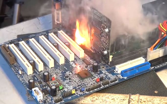
Breakdown Voltage is a critical parameter to consider. It is the maximum voltage that a material or PCB can withstand before it loses its insulating properties and begins to conduct. Once the breakdown voltage is exceeded, the PCB could experience catastrophic failure, with arcing between layers, damaged components, or even fire hazards.
Common High Voltage Applications
- Power electronics
- Medical devices
- Telecommunications
- Aerospace
- Electric vehicles (EVs)
- Military
- Industrial control system
- Communication
Best Technology make many high voltage PCBs for our customers, from industrial control PCB to aerospace, we have such experience in this area. If you have similiar projects, welcome to contact us.
You may also like


Tags: high voltage pcb, hv pcb