
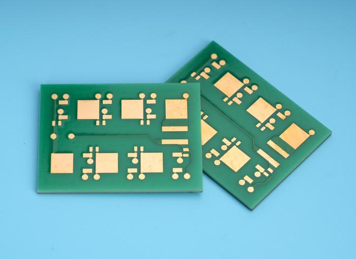
As an innovative technological achievement in the field of electronics, multilayer ceramic pcb are gradually becoming a key force in promoting the development of the electronics industry. It uses ceramic materials as substrates and integrates advanced printed circuit technology, providing solid support for the miniaturization and high performance of electronic equipment.
What is a multilayer ceramic pcb?
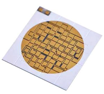
A multilayer ceramic pcb is an electronic component that uses ceramic as a matrix material and makes metal circuits on it. It is mainly divided into planar ceramic printed circuit boards and multilayer ceramic pcb.
Planar ceramic printed circuit boards are usually used in some simple electronic devices, while multilayer ceramic pcb are widely used in multiple high-end technology fields due to their higher integration and performance.
From a classification point of view, multilayer ceramic pcb can be divided from different angles. In terms of the number of layers, ceramic circuit boards are currently dominated by single and double panels.
According to materials, there are Al2O3 ceramics, AIN ceramics and BeO ceramics.
- Alumina substrates are commonly used substrate materials in the electronics industry, with high strength and chemical stability and abundant raw material sources.
- AIN ceramics have high thermal conductivity and expansion coefficients that match Si, but there are relatively few domestic production technologies and the price is high.
- Although BeO has high thermal conductivity, its development is limited by toxicity.
According to the manufacturing process, it can be roughly divided into four types: HTCC, LTCC, DBC, and DPC.
- DBC combines Al2O3 with Cu plate by high temperature heating.
- DPC deposits Cu on Al2O3 substrate by direct copper plating technology.
- LTCC is also called low-temperature co-fired multilayer ceramic substrate, and HTCC is also called high-temperature co-fired multilayer ceramic.
At present, these ceramic substrates have been maturely applied to various required fields, such as cooling sheets, high-power LEDs and other industries.
What are the manufacturing processes of multilayer ceramic pcb?
Common manufacturing processes of multilayer ceramic pcb:
- One-time sintering multilayer method: After the ceramic blank is stamped and formed, the conductive layer is printed, and then laminated or printed with an insulating layer, followed by shape punching, and finally sintered and plated with precious metals.
- Thick film multilayer method: After the ceramic blank is stamped and sintered, the conductive layer is printed, and the conductive layer and the insulating layer are printed repeatedly, and finally sintered.
- High temperature co-firing technology (HTCC): High temperature sintering is adopted, and the sintering temperature is usually above 1500℃. This technology can produce ceramic circuit boards with high mechanical strength, which can make the package more solid and durable. However, high melting metals such as tungsten, molybdenum, and manganese have poor conductivity and sintering shrinkage is difficult to control.
- Low temperature co-firing technology (LTCC): Sintering at 850-900 degrees Celsius, low-capacitance capacitors, resistors, coupling and other passive components are buried in the multilayer ceramic substrate, and low-impedance metals such as gold, silver, and copper are co-fired as electrodes, and then parallel printing is used to coat the circuit.
- Direct pressing technology (DBC): Al2O3 is combined with Cu plate by high temperature heating. The production process is relatively simple and direct, and ceramic circuit boards with certain performance can be quickly produced.
- Vacuum sputtering technology (DPC): Cu is deposited on Al2O3 substrate using direct copper plating technology, which can produce ceramic circuit boards with high precision.
What are the application fields of multilayer ceramic pcb?
(I) Covering high-end technology fields
multilayer ceramic pcb play a vital role in the aerospace field.
Ceramic materials do not decompose chemical bonds due to heat and ultraviolet radiation, do not absorb or release moisture in large quantities, and do not outgas in extreme vacuums. They have excellent temperature resistance and high reliability.
In satellite communication systems, navigation systems, and aircraft control systems, multilayer ceramic pcb ensure that circuits work stably in extreme environments.

In the field of medical equipment, multilayer ceramic pcb are widely used in imaging equipment and life support systems. The multilayer design can integrate more functions in a limited space, meeting the key needs of portable medical devices and compact designs.
In the field of automotive electronics, as cars develop towards electronicization and intelligence, the use of multilayer ceramic pcb is becoming more and more common. From engine management systems to entertainment systems, it improves circuit reliability, reduces weight, and improves overall performance.
In communication systems, especially in data centers and network equipment, multilayer ceramic pcb are widely used due to their superior signal integrity and electromagnetic interference shielding capabilities. High-speed signal transmission is possible while ensuring the quality and stability of data transmission.
In the field of high-performance computing, the high integration and high performance of multilayer ceramic pcb can meet the needs of large-scale data processing and high-speed computing.
(II) Significant advantages are widely used
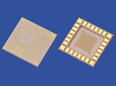
multilayer ceramic pcb have a high degree of integration and can arrange more components and circuits in a limited space to achieve more complex circuit designs.
It has extremely high reliability and adopts professional manufacturing processes with good electrical and mechanical properties. Through strict quality control and testing, the stability and reliability of the circuit board are guaranteed.
Strong design flexibility allows more complex circuit layouts, providing space for innovation and technological progress. Designers can optimize circuit design and reduce the length of signal paths, thereby speeding up signal transmission.
What are the unique advantages of multilayer ceramic pcb?
(I) Excellent performance
multilayer ceramic pcb have many excellent properties. First, high thermal conductivity enables them to dissipate heat quickly and effectively, ensuring that electronic components maintain a stable temperature during operation.
The good thermal expansion coefficient makes the thermal expansion coefficient of the ceramic circuit board similar to that of the chip, which can reduce the impact of thermal stress on the chip. When the temperature changes, the thermal stress between the circuit board and the chip is reduced, which improves the reliability and service life of the electronic equipment.
The low-resistance metal film layer ensures good conductivity and reduces the loss of signal transmission.
The substrate has good solderability, which is convenient for the installation and welding of electronic components and improves production efficiency. Good insulation can effectively prevent circuit short circuits and ensure the safe operation of electronic equipment.
The low high-frequency loss makes the multilayer ceramic pcb have significant advantages in the field of high-frequency communication. In high-frequency signal transmission, the signal loss is low, which can ensure the quality and stability of the signal.
The high-density assembly feature enables the ceramic circuit board to integrate more electronic components in a limited space and realize more complex circuit design.
(II) Rich types suitable for different scenarios
- Aluminum nitride ceramic circuit boards have the advantages of high thermal conductivity and expansion coefficient matching Si. Its high thermal conductivity can quickly dissipate the heat generated inside the device, making it an ideal packaging material for high-power electronic devices. In the field of high-power LED lighting, aluminum nitride ceramic circuit boards can provide good heat dissipation performance and extend the service life of LED lamps.
- Alumina ceramic circuit boards are more common, cost-effective, with good insulation and moderate thermal conductivity. Alumina substrates are commonly used substrate materials in the electronics industry, with high strength and chemical stability, abundant raw material sources, and are suitable for a variety of technical manufacturing and different shapes.
- Thick film ceramic circuit boards consist of gold and dielectric paste printed on a ceramic substrate and baked at a temperature slightly below 1000°C. Thick film ceramic PCBs can use gold or copper, and copper is used most due to its lower cost.
- LTCC has excellent high frequency, high Q characteristics and high-speed transmission characteristics, good temperature characteristics, can adapt to high current and high temperature resistance requirements, easy to achieve multi-functionality and improve assembly density, and high reliability.
- High temperature co-fired ceramic (HTCC) circuit boards use alumina and adhesives as well as plasticizers, solvents and lubricants. This method is most suitable for small circuit boards and carrier circuits. HTCC has the advantages of high mechanical strength, high wiring density, and stable chemical properties.
What is the future development of multilayer ceramic pcb?
(I) The market size continues to grow
In recent years, the market size of my country’s ceramic circuit board industry has shown a trend of continuous growth. According to statistics, the market size will be about 2.399 billion yuan by 2023, and the CAGR from 2015 to 2023 will be 19.1%. With the continuous development of the electronic information industry, the market demand for ceramic circuit boards as key electronic components will continue to grow.
(II) Technological progress drives development
With the rapid development of the new generation of information technology, downstream demand will inevitably be more diversified and more technologically advanced, which will put forward higher requirements on the R&D level and process level of ceramic circuit board industry manufacturers.
The downstream industries include integrated circuit packaging, LED, automotive electronics, aerospace and military electronic components. The scale development of the downstream market has created considerable new market capacity for the ceramic circuit board industry. At the same time, the structural upgrading of the downstream industry will help the technological progress of the ceramic circuit board industry.
(III) The global market has broad prospects
In 2023, the global multilayer printed circuit board market size is about 168.8 billion yuan, and it is expected that the market size will be close to 192.9 billion yuan by 2030, with a CAGR of 1.9% in the next six years.
At present, China is the world’s largest market for multilayer printed circuit boards, accounting for nearly 60% of the market share. From the perspective of the global market competition landscape, the sales volume, revenue, price market share and industry ranking of multilayer printed circuit boards of leading companies in the global market are constantly changing.
Conclusion:
In short, multilayer ceramic pcb have shown great potential in the electronics industry with their unique advantages. With the continuous advancement of science and technology, it will play a more key role in more fields and continue to inject new vitality into the innovation and development of electronic technology. BEST Techbology has always been committed to providing customers with high-quality products and professional services, and continuously promoting the development of the ceramic circuit board industry.
You may also like


Tags: ceramic PCB, multilayer ceramic pcb, PCB, pcb design