
What is pcba?
PCBA is the abbreviation of Printed Circuit Board Assembly, which means “circuit board assembly” or “circuit board assembly”. It refers to installing electronic components on a printed circuit board and connecting the components to the circuit board through welding and other methods to form a complete circuit system.
This process involves multiple important links, including SMT (surface mount technology) mounting, DIP (dual in-line package) plug-in, etc., which eventually form a key component of electronic products. PCBA is not only the physical support of electronic equipment, but also provides a way to connect circuits, and also plays a role in protecting components and dissipating heat. In the manufacturing process of electronic products, the production process of PCBA includes steps such as PCB design, manufacturing, component placement, welding and testing to ensure the functionality and reliability of the product.
What does pcba stand for in electronics
PCBA stands for Printed Circuit Board Assembly in electronic products. PCBA is the process of assembling and soldering electronic components on a printed circuit board to form a complete circuit board. It is an important part of modern electronic products, including mobile phones, computers, cars, home appliances, etc.
. PCBA processing involves several important links, such as SMT (surface mount technology) and DIP (dual in-line package) plug-ins, which ensure the correct placement of electronic components and the reliability of the circuit. In addition, the use of PCBA processing equipment and the improvement of manufacturing processes, such as printers and dispensing machines, have improved the yield and efficiency of PCBA processing products
What is pcba manufacturing
The manufacturing process of PCB (printed circuit board) involves multiple process links, including design, plate making, drilling, filling, electroplating, etc. These steps together constitute the manufacturing process of PCB.
- Design: First, according to the needs and layout design of the circuit, the circuit diagram is drawn using computer-aided design (CAD) software. This stage is very critical because it directly determines the function and performance of the PCB.
- Plate making: After the design is completed, the designed circuit diagram needs to be converted into a practical PCB board that can be made. This usually involves the use of photosensitive materials and special chemical treatments so that the circuit pattern can be accurately transferred to the PCB substrate.
- Drilling: After the plate making is completed, holes need to be drilled on the substrate according to the designed circuit pattern. These holes are used for subsequent wiring connections. The precision and accuracy of drilling are essential to ensure the normal operation of the circuit.
- Filling: After drilling, some substances, such as resin, need to be filled in the hole to enhance the structural strength and electrical insulation performance of the PCB.
- Electroplated: In order to ensure good electrical connection, the PCB needs to be electroplated, usually by electroplating a layer of copper or other conductive materials on the copper foil. This step is very important to ensure the conductivity and durability of the circuit.
- Lamination and cutting: After the electroplating is completed, the multi-layer circuit boards are laminated together to form a multi-layer PCB. Subsequently, the PCB boards are cut into specific sizes as needed.
- Inspection and testing: The manufactured PCB is inspected and tested to ensure that its functions and performance meet the design requirements. This may include visual inspection, functional testing and other methods.
- Finished product assembly: The qualified PCBA board is assembled into the shell
What is the SMT process in PCBA?
1. Programming and adjusting the SMT machine: According to the information provided by the customer, program the coordinates of the location of the SMT components and perform the first piece check.
2. Printing solder paste: Use a screen printer to print the solder paste on the pads on the PCB board where the electronic components need to be soldered.
3. SPI inspection: Use a solder paste detector to detect the quality of solder paste printing to ensure that there are no defects.
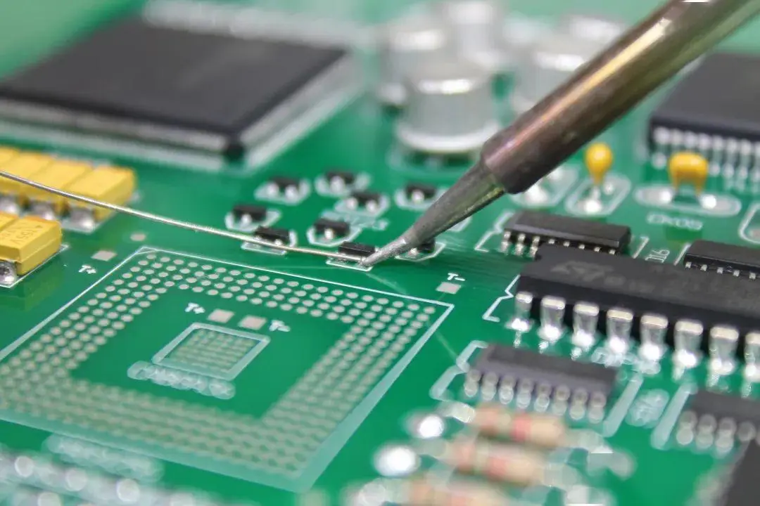
4. SMT: Use a SMT machine to accurately install the electronic components SMD to the fixed position of the PCB.
5. High-temperature solder paste melting: The solder paste is melted at high temperature through a reflow oven to firmly solder the electronic components SMD and the PCB board together.
6. AOI inspection: Use an automatic optical inspection instrument to detect whether the PCBA components after welding have poor welding.
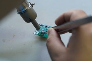
7. Visual inspection: Manual inspection checks the version of the PCBA, whether the direction of the components is correct, and the defects after welding.
8. Packaging: The qualified products are separated and packaged. The packaging materials used include anti-static bubble bags, static cotton, blister trays, etc.
PCB Assembly manufacturer High Quality & Fast Delivery
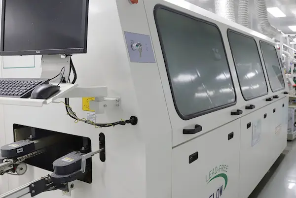
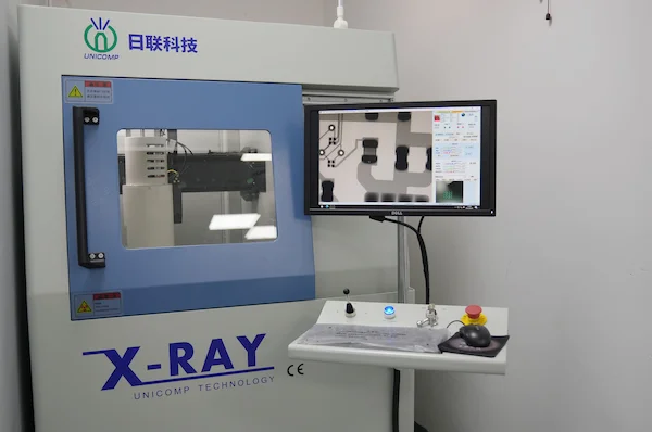
Best Technology is a PCB assembly manufacturer in Asia, who specializes in printed circuit board assembly (PCBA) and manufacturing. We have our own PCBA factory with 8 SMT lines, each line equipped with full-automated manufacturing and testing machine. In our PCBA factory, you can see dual-online AOI, SPI, X-RAY, nitrogen reflow oevn and so on. We are certified by ISO9001, ISO13485, and IATF16949, ensuring the highest quality standards in every PCB project.
Full turnkey service from pcb design, pcb manufacturing, component sourcing, pcb assembly, pcb duplicating in a very short time.
We source all the parts directly from the manufacturers or from authorized distributors such as Digikey, Mouser,Future,TTI,Avnet and Arrow to avoid counterfeit parts.
We also warehouse a significant inventory of common parts.If we cannot source a specific component, our engineers will make recommendations for fair-price alternatives.
What is pcba test
PCBA testing is the process of testing the electrical conductivity and input-output values of the PCBA circuit board with mounted electronic components to ensure that all the installed circuit boards are completely consistent with the various specifications and parameters of the design. Through strict testing, the performance and reliability of the PCBA board can be improved, customer trust can be won, and cooperation between enterprises and customers can be promoted.
PCBA testing includes various test forms, such as ICT testing (internal circuit testing), FCT testing (functional testing), fatigue testing, extreme environment testing and aging testing.
ICT testing tests the characteristics of devices and circuit networks by applying test probes to the test points on the PCB.
FCT testing is mainly used to test the electronic and electrical functional aspects of the PCBA board, and is tested under the condition of simulating the actual operating state of the PCBA board. Fatigue testing performs high-frequency and long-term operations by sampling to observe whether failures occur.
Extreme environment testing places the PCBA board in harsh and extreme environments, such as high temperature, severe cold, and falling, to infer the reliability of the PCBA board. Aging testing is to power on the PCBA board and electronic products for a long time to observe whether any failures occur.
What is a pcba number
A combination of letters and numbers used to uniquely identify and track each electronic component on a circuit board. These numbers are often called component numbers, part numbers, or reference designators.
On PCBA boards, the format and meaning of these numbers may vary depending on the manufacturer and designer, but generally follow certain rules.
For example, common numbers are R107, C118, Q102, D202, etc., where:
The first letter usually identifies the type of device, such as: R for resistors, C for capacitors, D for diodes, Q for transistors, etc.
The subsequent digital part may indicate the circuit function number (such as “1” may indicate the motherboard circuit, “2” may indicate the power supply circuit, etc.) and the serial number of the device on the circuit board.
FAQ About PCBA
hat does poor welding include and what kind of faults will it cause?
Poor welding is manifested as incomplete solder joints, cold solder joints, etc., which lead to reduced conductivity of the circuit board or circuit failure. Solutions include optimizing soldering parameters, ensuring pad cleanliness, adjusting soldering energy, and increasing soldering temperature or extending soldering time.
What causes component misalignment?
It is caused by inaccurate positioning of components during the soldering process, affecting circuit connection and product function. Solutions include implementing precise visual inspection and automatic inspection to ensure that components are placed correctly and rework and repair.
What do short circuits and open circuits mean?
Short circuits and open circuits: caused by poor insulation or fracture between adjacent solder joints on the circuit board or between solder joints and lines, which may cause abnormal current flow or circuit interruption. Solutions include ensuring that solder paste is evenly applied, components are correctly placed, and adjusting soldering parameters to avoid excessive soldering temperature and pressure.
What causes solder cracking?
Solder cracking: cracking occurs during use or after a certain environmental stress, usually due to excessively high temperatures, long soldering time, or improper selection of soldering materials during the soldering process. Solutions include optimizing soldering parameters, ensuring proper soldering temperature and time, and selecting appropriate soldering materials.
Why electrostatic discharge?
Electrostatic discharge (ESD) damage: Sensitive electronic components can be damaged by ESD. Solutions include implementing ESD control measures in the production environment, such as using ESD gloves and anti-static workbenches.
Does voltage instability affect PCBA performance?
Power supply issues: Power supply stability issues can affect PCBA performance. Solutions include implementing power electronics technology and voltage regulators to ensure stable power supply.
what does pcba stand for
PCBA stands for Printed Circuit Board Assembly. Other synonyms of PCBA include “PCB Assembly”, “Populated PCB” and “Board Assembly”. These terms are widely used in the electronics industry to describe the finished or semi-finished state of a circuit board after component placement and soldering.
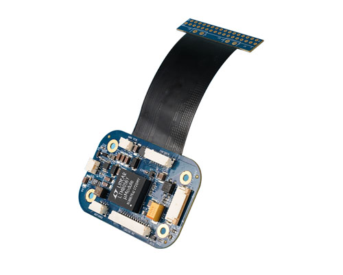
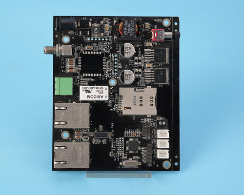
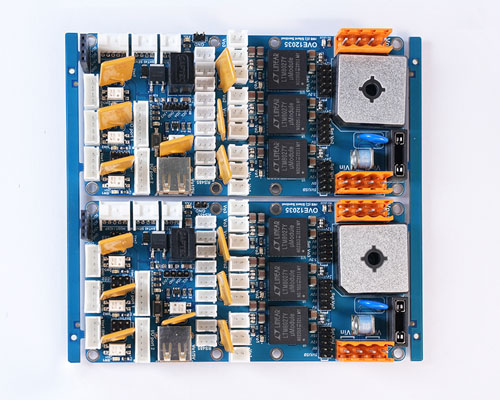
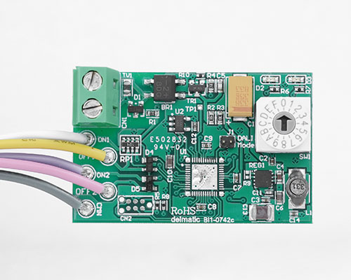
what is a pcba board
PCBA board, full name Printed Circuit Board Assembly, Chinese name is printed circuit board assembly, refers to the installation and welding of components on the completed printed circuit board to form a circuit board that can be used directly.
The production process of PCBA board mainly includes three steps: component mounting, welding and testing. First, the obtained components are accurately positioned and mounted on the PCB board according to the design requirements, and then the components are firmly fixed on the PCB board by welding, and the circuit is ensured to be unobstructed. Finally, the circuit is tested to verify whether it is working properly. The whole process requires a high degree of technology and precision to ensure the quality of PCBA board.
You may also like


Tags: PCB Assembly manufacturer, PCBA