
What file type is used for pcb designs?Generally, PCB boards require Gerber files, drilling files, bill of materials (BOM), manufacturing drawings and assembly drawings. The Gerber file suffix is .gbr, the drilling file suffix is (.drl), and the PCB schematic file suffix is .schdoc. The drilling file is usually in Excellon format (.xin). The center coordinate file is also called the pick and place file, which is provided in CSV (comma separated value) format.
Whether it is an individual or a company making PCB boards, PCB boards generally require Gerber files, drilling files, bill of materials (BOM), manufacturing drawings and assembly drawings. Among them, Gerber files are a set of files, which are the most important and contain information about each layer of the PCB to be used in production.
What files do I need to make a PCB?
Making PCBs (printed circuit boards) requires a series of files to ensure the smooth progress of the manufacturing process and the quality of the product.
Gerber file: This is the most common and crucial file in PCB manufacturing. It contains the geometric information of each layer of the PCB, such as copper lines, pads, solder mask layers and silk screen layers, and also includes separate files for each PCB layer, such as top copper, bottom copper, solder mask, silk screen layer, etc.

Drill file: Provides drilling coordinates and size information for PCBs, and specifies the aperture size of components, vias and mounting holes. Drill files are usually generated in Excellon format or as separate ASCII files.
Bill of Materials (BOM): A BOM is a detailed list of all components used in a PCB design, including information such as part number, component value, description, and quantity, which helps ensure that all required components are correctly sourced and placed on the PCB.
Center Coordinate File: Also known as a pick and place file, it provides coordinate and orientation information for each component on the PCB and is essential for the automated assembly process. Center coordinate files are usually provided in CSV format.
Fabrication Drawing: This is an engineering drawing that includes key information about the PCB, such as board dimensions, drill hole dimensions, layer stackup, tolerances, surface finish, and other manufacturing-related details, which serves as a reference for PCB manufacturers during the production process.
Assembly Drawing: Provides additional information for the PCB assembly process, including component placement details, reference numbers, orientation, and any special instructions for assembly technicians.
In addition, depending on the specific design and production needs, other documents may also be required, such as circuit diagrams, special layer files, installation instructions and precautions, etc. The preparation and provision of these documents is a key step in ensuring a smooth PCB production process.
What are Gerber files? What information do they contain?
Gerber files are a series of ASCII vector format files that define PCB design specifications. They are generated using electronic design automation (EDA) or computer-aided design (CAD) tools and provide information such as board configuration parameters, aperture descriptions, XY coordinate locations, and drawing instructions.
Configuration details include the size and shape of the PCB to be manufactured. Each layer of the board information is recorded in a different file to define components such as copper traces, pads, vias, solder mask, silk screen, and logos. The Gerber file indicates the XY coordinate location of each geometric shape and uses instructions to draw these shapes on the physical board.
The basic components of the Gerber file include: board size, shape, top assembly, top silk screen, top solder mask, top paste, top copper, internal signals, inner layers, bottom copper, bottom paste, bottom solder mask, bottom silk screen, bottom assembly, and manufacturing information (providing stackup, drilling details, cutting, etc.).
Gerber files generated by computer-aided manufacturing (CAM) tools have user-selected extensions, usually using project naming such as “.TOP” for top layer, “.BOT” for bottom layer, and “.drl” for drill data.
How is a PCB designed?
PCB design is a complex process that involves multiple steps and considerations to ensure the functionality and reliability of the final product.
Schematic Design: First, you need to prepare a schematic and component library. The schematic is the blueprint of the circuit design, while the component library contains information about the various components used in the circuit.
Component Symbols and Packages: The symbol of the component is used to represent the component in the schematic, while the package defines the physical form of the component on the PCB. The component symbol is used in the schematic design stage, while the package is used in the PCB layout and routing stages.
How is a PCB designed?
PCB Layout: The layout stage involves placing electronic components on the PCB, and factors that need to be considered include the orientation, size, and relative position of the components.
Routing: After the layout is completed, the next step is the routing stage, which is to connect the various components according to the needs of the circuit.
DRC Check: Design rule checking (DRC) is performed during the design process to ensure that the design complies with predetermined electrical and physical rules. This includes checking for shorts, open circuits, and other possible design errors.
Solder mask and solder paste layer: The solder mask is used to prevent unnecessary soldering, while the solder paste layer is used to specify solder joints. The correct design of these layers is critical to ensuring the reliability and manufacturability of the circuit board.
Network and DRC Check: In the final stage of design, network checks are performed to ensure that all components are properly connected, while DRC checks are performed to verify that the design complies with all electrical and physical rules.
Through the above steps, designers are able to transform the circuit design in the schematic into an actual, manufacturable PCB. This process requires comprehensive consideration of multiple factors such as the functionality, reliability, and manufacturing cost of the circuit.
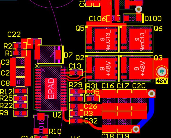
What is the schematic file for PCB?
PCB schematic files are the main files used for circuit design, analysis, and debugging. They mainly show the electrical connection relationship between electronic components, but do not reflect the actual physical location of these components on the PCB board.
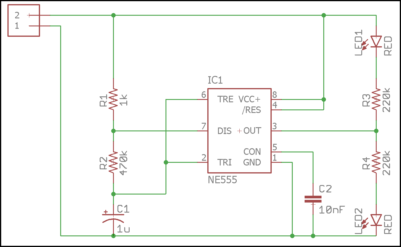
Schematic Diagram is the basis of circuit design. It uses symbols and lines to express the connection and working principle of the circuit in a concise and clear manner, and pays more attention to the functional expression of the circuit.
Schematic diagram does not involve the specific layout and wiring of electronic components on the PCB board, so it focuses on the logical representation of the circuit rather than the physical implementation.
In contrast, PCB design files plan the precise location and wiring of electronic components on the PCB board in detail, taking into account the connectivity of the circuit, and also comprehensively considering factors such as signal integrity, power distribution, thermal design, and mechanical strength.
These design files are the main files used to manufacture actual electronic devices, including PCB layout and PCB wiring. The layout determines the location of electronic components on the circuit board, while the wiring involves the electrical connection between components.
In general, schematic files and PCB design files play different roles in the design and manufacturing process of electronic products. The former focuses on the expression of circuit logic and function, while the latter focuses on converting this logic into actual physical implementation, including the specific location and connection method of components.
What is the difference between PCB design and schematic design?
The main difference between PCB design and schematic design lies in their purpose, content and application scenarios.
Purpose and content:
Schematic design focuses on describing the logical relationship and electrical performance of the circuit, using graphic symbols to display power, components and connections, and can clearly show the logical relationship of the internal circuit of the electronic device. It is mainly used for circuit analysis and design, helping to understand the working principle of the equipment and perform fault diagnosis.
PCB design focuses on describing the actual physical size, position and wiring of components, and is the actual circuit board layout and wiring design based on the schematic diagram. It is mainly used to guide the manufacture and assembly of PCBs, reflecting the actual layout and wiring of electronic equipment.
Application scenarios:
Schematic design plays an important role in the process of R&D, debugging and maintenance, and is a key tool for understanding the working principle of the equipment and performing fault diagnosis.
PCB design files are an important basis for the actual PCB board manufacturing and subsequent assembly, debugging and other processes.
In short, schematic design is the basis of electronic product development. It provides information such as the logical relationship and electrical performance of the circuit, while PCB design is the key link to convert the schematic into an actual circuit board. It is necessary to design components layout and wiring according to the requirements of the schematic.
What is a PCB stencil file?
A PCB stencil file is a pre-designed file template used to quickly generate PCB design files containing specific information.
These template files usually contain basic information such as board size, board layer settings, grid settings, and title bar settings. Users can quickly generate new PCB design files based on these templates, thereby speeding up the design process.
By using these templates, designers can avoid designing these basic settings from scratch, saving time and energy, and focusing on more complex circuit design details.
Conclusion:
There are many types of PCB design files, among which Gerber files are the most important. The information they contain is the most and the most important. The final quality of the PCB circuit board depends on the first step of design. BEST Technology has very professional PCB designers who have many years of industry experience and can meet all your needs.
You may also like


Tags: PCB, pcb design, PCBA, printed circuit board