

What is a Pinner in PCB?
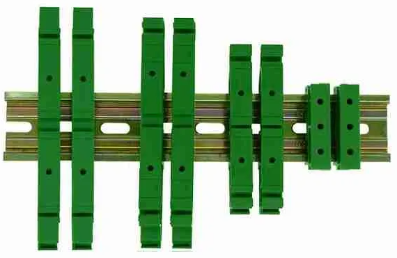
What is a Pinner in PCB? A Pinner in PCB manufacturing is a specialized tool or mechanism used to align and secure various components or layers during the assembly process of printed circuit boards (PCBs). It ensures that all elements, whether they are individual electronic components or stacked layers in multilayer boards, remain accurately positioned until the final bonding or soldering process is completed. In simple terms, it acts as a “placeholder,” holding everything firmly in place to avoid any shifts or misalignments that could compromise the performance or quality of the PCB.
Pinners can be manual, semi-automatic, or fully automated, depending on the scale and precision requirements of the production line. While manual pinners are often used for small-scale production or prototypes, automatic pinners are prevalent in large-scale manufacturing due to their high efficiency and accuracy.
Function of PCB Pinner
The function of a PCB pinner is primarily to align and secure PCB layers or components during the assembly process, ensuring that everything is held in place precisely before final soldering or bonding. Here’s a breakdown of its essential functions:
1. Component Placement Stability
One of the key functions of a PCB pinner is to provide stability to the components placed on the PCB. Whether it is a surface-mounted component, a through-hole part, or different layers in a multilayer PCB, the pinner holds these elements firmly in place to prevent any shifting during further processes such as soldering, wave soldering, or selective soldering.
2. Accurate Layer Alignment
In multilayer PCB manufacturing, aligning the various layers accurately is a complicated but crucial task. A pinner ensures that each layer is positioned perfectly over the others, preventing any misalignment that could result in short circuits, poor signal transmission, or weak connections between layers. In multilayer PCBs, where hundreds of traces may overlap in different layers, alignment is critical to ensure the board functions correctly.
3. Minimization of Errors
Errors such as misaligned components or layers can lead to significant issues like short circuits or signal interference in PCBs. By keeping everything in place with high precision, the PCB pinner reduces the chances of human or machine errors during assembly.
4. Support During Automated Processes
In automated assembly lines, the PCB pinner often works in coordination with other machines such as pick-and-place machines and soldering stations. While components are being positioned by a robotic arm or soldering is taking place, the pinner ensures that none of the components shift out of alignment.
5. Enabling High-Density PCB Designs
As PCB designs become more complex and denser with miniaturized components, the risk of misalignment increases. A pinner helps overcome this challenge by holding even the smallest components in the exact position, preventing misplacement in densely packed circuits.
6. Enhancing Overall Manufacturing Efficiency
Using a pinner enhances the overall efficiency of the manufacturing process. It allows other automated systems to perform their functions more swiftly because there’s less risk of a production halt due to misaligned components.
7. Reducing Rework and Scrap
The precision offered by PCB pinners means there are fewer instances of defective boards, which in turn means less rework and lower scrap rates. By ensuring proper alignment, pinners contribute to a higher yield of functional PCBs, reducing the amount of waste produced during manufacturing.
Types of PCB Pinner
The selection of a PCB pinner depends on the specific requirements of the assembly process, the type of components being used, and the complexity of the PCB design. Below are some common types of PCB pinners:
Through-Hole Pinners
These are designed for use in through-hole PCB assembly, where components have leads that pass through holes in the board. Through-hole pinners secure these leads in place, ensuring they remain stable during the soldering process. They are especially useful for components with multiple leads, such as integrated circuits.
Surface Mount Pinners
Surface mount technology (SMT) is a widely used method for mounting components directly onto the surface of a PCB without the need for leads to pass through the board. Surface mount pinners are specifically designed to hold these components in place on the board’s surface, preventing movement during reflow soldering.
High-Precision Pinners
Certain PCB assemblies require extremely high precision, especially in fields like aerospace or medical devices. High-precision pinners are engineered to hold components with micron-level accuracy, ensuring even the slightest misalignment is avoided. These pinners are often used alongside advanced placement machines that demand exact component positioning.
Custom Pinners
In some cases, standard pinners may not meet the unique needs of a specific PCB assembly process. Custom pinners can be designed and manufactured to accommodate specialized component shapes, board layouts, or particular assembly requirements. These pinners are typically developed through collaboration between PCB designers and pinner manufacturers to meet the exact specifications of the production line.
How Does a PCB Pinner Work?
A PCB pinner works by using pins or clamps to hold the PCB layers or components in place during the assembly process. When layers of a PCB are stacked or when components need to be placed with high precision, the pinner ensures they remain aligned. The pins are positioned strategically to avoid any areas where components will be placed or where soldering will occur. Once the components are secure, the pins can be removed without disturbing the alignment, leaving the PCB ready for soldering or bonding.
In automated systems, the pinner operates in sync with other assembly tools, such as pick-and-place machines or soldering stations, making the entire process seamless and highly efficient.
Advantages of Using PCB Pinner
There are several key advantages to using a PCB pinner in the manufacturing process:
1. PCB pinners ensure that all components and layers are perfectly aligned, reducing errors that could lead to faulty boards.
2. By securing the components, the pinner allows other machines to work faster without the risk of misalignment, speeding up the overall assembly process.
3. A well-aligned PCB means fewer errors and less rework. This not only saves time but also reduces material waste and associated costs.
4. Consistently aligned components lead to more reliable PCBs, which translates into higher product quality and fewer defects.
5. PCB pinners can be used with various PCB types, including single-layer, multilayer, and flexible PCBs.
What is Pinner in PCB Factory?
In a factory setting, where large volumes of PCBs are produced, PCB pinners are often integrated into the assembly line as part of a highly automated process. These pinners work in conjunction with other assembly machines, such as pick-and-place machines and soldering stations, to create a streamlined manufacturing process. By securing the PCB layers or components in place, pinners prevent shifts that can occur due to vibration, movement, or machine interaction, ensuring that the assembly process proceeds without errors.
In sectors where precision is vital, such as aerospace, automotive, medical devices, and telecommunications, even the slightest misalignment can lead to failure or reduced performance. PCB factories that operate in these high-precision fields rely heavily on pinners to ensure that all components are perfectly placed and secured before final assembly. The reliability and quality of the final PCB often depend on how well the pinner performs its job in maintaining alignment throughout the process.
Tags: pcb pinner