

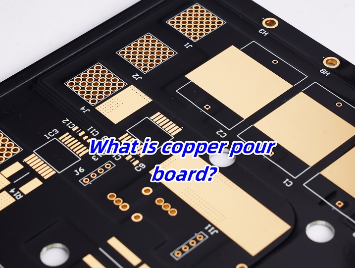
What is Copper Pour in PCB Design?
Copper pour, also known as copper coating, refers to filled solid copper on PCB where without trace layout area or idle space. Instead of leaving unused areas bare, copper is poured over them, connecting it to the ground or other designated signals. The main purpose of this process is to reduce the ground impedance, improve the anti-interference ability, reduce the voltage drop. Thereby improving the power supply efficiency, and connect with the ground wire to reduce the loop area. By covering large sections of the board with copper, it also minimizes signal interference and adds a layer of protection to the PCB. Copper pour are essential for designers to maintain signal integrity and reduce unwanted noise.
The process of copper coating is not only very important for digital circuits, because it can effectively reduce the ground impedance, which is particularly important for digital circuits with a large number of spiking pulse currents. However, for analog circuits, the ground wire loop formed by laying copper may cause electromagnetic coupling interference.
Why Use Copper Pours on Circuit Boards?
Copper pours offer several advantages that make them an essential part of circuit board design. When creating PCBs, some engineers tend to leave many copper-free areas on the board. But a high percentage of copper-free areas on the PCB can negatively affect the product, making it vulnerable to early damage, when copper pouring comes in handy.
There are some novices who think that less copper pouring means that the cost will be lower and lower, which is wrong. It is true that the plating area is small, which can save copper, but there is no way to guarantee the quality, and the appropriate amount of copper pouring can improve the quality of the product.
When the PCB board is placed in the plating tank and the appropriate current is applied, the PCB will show the physical state after dry film coverage. After passing a current, the circuit lines exposed to the outside of the dry film will be plated with copper from the plating tank. The total area of the part of the circuit exposed outside the dry film will affect the value of the current distribution during the plating process, if the bare copper area is large, the current input is uniform, and the current received is more uniform. Therefore, a large area of copper plane must be laid in the design to prevent this from happening. If the total plating area of copper is too small or the pattern distribution is very uneven, the received current will not be uniform. In this way, when powered on, the greater the current, the thicker the copper plating layer (so designed, if only 1OZ is required, then the finished copper thickness can reach 2OZ).
If the gap between current traces is too small, for example about 3mil to 3.5mil, a “clip film” will form between the traces. In other words, the dry film is caught in the middle of the gap, which causes the subsequent base to start the copper in the middle, which can lead to a short circuit if the etching process is not cleaned. In order to maintain the high quality of PCB manufacturing, independent lines must be avoided as much as possible in PCB design and layout. In addition, it is recommended to use a large amount of copper on the entire PCB, if there is a separate line that cannot be covered with copper, then the continuation between the lines must be as wide as possible.
Advantages of Copper Pour Board
1. For EMC (electromagnetic compatibility) requirements, a large area of ground or power supply needs to be covered with copper, which will play a shielding role. For some special area, such as protective ground, it plays a protective role.
2. From PCB manufacturing perspective, generally in order to ensure an uniform copper plating, or avoid lamination deformation and bending, manufacturers always pour copper for those less trace layout PCB board.
3. For signal integrity PCB, pour copper gives the high-frequency digital signal a complete return path, and reduce the wiring of the DC network. In another way, pour copper can help to heat dissipation.
Disadvantages of Copper Pour
1. If the pins of the components are fully covered with copper, the heat dissipation may be too fast, resulting in difficulties in dismantling and repairing the components. Therefore, sometimes in order to avoid this situation, cross connections are used for components (pin contact and pad contact are shown in “+”).
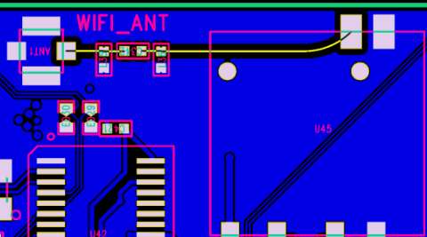
2. Pouring copper in the area around the antenna is easy to cause weak signal, interfered acquisition signal, and the impedance of copper will affect the performance of the amplifier circuit. So the area around the antenna section is usually not covered with copper.
Copper Pour vs Ground Plane
There’s often confusion between copper pours and ground planes. While both serve similar purposes, they are not the same. A ground plane is a layer dedicated entirely to the ground signal, covering the entire surface of a board layer. It ensures a low-impedance path for electrical signals, minimizing interference.
Copper pours, on the other hand, are not necessarily tied to the ground. Designers can connect copper pours to any net, including power lines or signal traces. The primary goal of a copper pour is to fill in empty spaces, whereas a ground plane is dedicated exclusively to providing a ground connection.
Implementation of PCB Copper Pours
When designing a PCB with copper pours, a few best practices help in optimizing its performance. Here are some useful tips:
- Assign Copper Pours to Ground First
When designing, prioritize assigning continuous copper to ground layers over power planes. A solid ground plane improves overall performance, providing a reliable reference for signals and reducing noise. Every PCB should have strong, consistent ground connections.
- Monitor Trace Currents
Although reducing inductance is advantageous, flooding the board with copper can sometimes interfere with circuit tuning. Be mindful of traced paths, especially in high-current areas, to maintain proper load control.
- Maintain Symmetry in Copper Pours
Ensure copper pours are symmetrical on both sides of the PCB. This balance helps prevent issues like board warping due to uneven expansion or moisture absorption. Symmetrical copper distribution is essential for the board’s structural integrity.
- Avoid Acute Angles
Keep copper pours free from long, narrow protrusions or angles sharper than 45 degrees. Such shapes can become weak points, breaking off or acting as antennas during vibration or shock, potentially causing functional failures.
- Incorporate Relief Features
Adding slots, anti-pads, and thermal spokes can relieve stress caused by material expansion, especially for large copper pours used on power planes. These features ensure mechanical stability and ease soldering.
- Carefully Review Design Masks
Automated copper pour shapes may need manual adjustments to remove artifacts or undesirable patterns around complex components. Always review and fine-tune these masks to achieve optimal results.
When copper pours are correctly connected to appropriate nets, designers can enhance both the electrical and physical properties of the circuit by distributing copper strategically across the board.
Copper Pour Clearances and Settings
When designing a PCB with copper pours, clearances and settings play a crucial role in ensuring proper functionality and avoiding issues like short circuits. Here are PCB copper pour suggestions based on standard PCB board:
1. Trace to Copper Pour Clearance
- Standard clearance: 0.2 mm (200 µm) or 8 mils
- High-voltage applications: 1 mm (1000 µm) or 40 mils (or more, depending on voltage levels)
2. Pad to Copper Pour Clearance
- SMD pads: 0.2 mm to 0.3 mm (8-12 mils)
- Through-hole pads: 0.3 mm to 0.5 mm (12-20 mils)
You can adjust these values based on the pad size and the net to which the copper pour is connected.
3. Copper Pour Width and Thickness
The width and thickness of the copper pour should be chosen based on the current-carrying capacity of the board:
- Minimum width: 1.5 mm (60 mils) for low-current signals
- Power lines: At least 2-3 mm (80-120 mils), depending on current
- Copper thickness: 35 µm (1 oz/ft²) is standard, but for higher currents, you can use thicker copper like 70 µm (2 oz/ft²) or more.
4. Via Clearance in Copper Pours
- Standard via clearance: 0.2 mm (8 mils)
- High-current via clearance: 0.5 mm (20 mils)
Clearance should be adapted to the board’s layer stack-up and current needs.
5. Thermal Relief Spokes
- Spoke width: 0.3 mm to 0.5 mm (12-20 mils)
- Spoke count: Typically 4 thermal relief spokes per pad
- Clearance to pad center: 0.5 mm (20 mils)
6. Copper Pour to Board Edge Clearance
- Standard clearance: 0.5 mm (20 mils) from the board edge
- High-voltage boards: 1 mm (40 mils) or more
Layer Placement of Copper Pours
Copper pours can be placed on any layer of a PCB. In multi-layer PCBs, copper pours are often added on internal layers to maximize performance. For example, ground and power pours are frequently found on internal layers to reduce noise and improve thermal dissipation.
On outer layers, copper pours serve to enhance thermal management. They distribute heat from high-power components and help maintain an even temperature across the board. It’s important to balance the placement of copper pours with other components to ensure overall board stability and functionality.
Copper Pour PCB Design Considerations
1. The open areas in the design must be minimized and the open Spaces filled with copper.
2. It’s important to assess the current-carrying capacity. Make sure the copper pour is thick enough to handle the expected current loads, especially in power applications.
3. If there is no room for the copper, the two wires, the two pads, and the distance between the wires and the pads are designed to be 2 ounces thick with a minimum spacing of 8 mil.
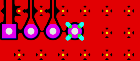
4. When pouring copper, keep a certain distance from the ordinary touch pad. The distance between the track, the common plane and the drilled area should be greater than 0.5 mm. The copper must be poured as firmly as possible. Avoid pouring copper on small grids.
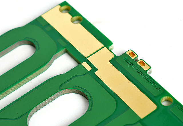
5. The inner layer of the gold finger must be all poured copper to avoid thinning of the board at the gold finger. Avoid choosing laminated structures with thin plates.
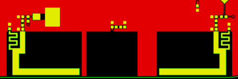
6. Those thin long, poorly grounded ground copper will have an antenna effect, which will cause poor EMC problems. Therefore, we should try to avoid causing broken copper when coating copper, such as causing broken copper can be removed.
7. Isolated (dead zone) copper problem, isolated copper if relatively small equivalent to broken copper can be deleted. If it is large, it can be defined as a place to add through the hole treatment, at this time there is no isolated copper.
8. Refer to the product design manual and apply copper coating near the antenna. Any interference or interference with the antenna must be avoided when pouring fake copper.
Tags: copper pour pcb, pcb design, pour board